Milestone-Proposal:Thin Film Hall Elements
To see comments, or add a comment to this discussion, click here.
Docket #:2025-19
This proposal has been submitted for review.
To the proposer’s knowledge, is this achievement subject to litigation? No
Is the achievement you are proposing more than 25 years old? Yes
Is the achievement you are proposing within IEEE’s designated fields as defined by IEEE Bylaw I-104.11, namely: Engineering, Computer Sciences and Information Technology, Physical Sciences, Biological and Medical Sciences, Mathematics, Technical Communications, Education, Management, and Law and Policy. Yes
Did the achievement provide a meaningful benefit for humanity? Yes
Was it of at least regional importance? Yes
Has an IEEE Organizational Unit agreed to pay for the milestone plaque(s)? Yes
Has the IEEE Section(s) in which the plaque(s) will be located agreed to arrange the dedication ceremony? Yes
Has the IEEE Section in which the milestone is located agreed to take responsibility for the plaque after it is dedicated? Yes
Has the owner of the site agreed to have it designated as an IEEE Milestone? Yes
Year or range of years in which the achievement occurred:
1983
Title of the proposed milestone:
Commercialization of Thin Film Hall Elements, 1983
Plaque citation summarizing the achievement and its significance; if personal name(s) are included, such name(s) must follow the achievement itself in the citation wording: Text absolutely limited by plaque dimensions to 70 words; 60 is preferable for aesthetic reasons.
In 1983, Asahi Kasei commercialized thin-film Hall elements, revolutionizing magnetic sensing. These sensors, based on the Hall effect, featured a novel structure with thin-film InSb sandwiched between ferrites, significantly enhancing sensitivity and temperature characteristics. Their high performance enabled widespread adoption in consumer and industrial electronics. This innovation marked an important milestone in the development of semiconductor-based thin-film magnetic sensors.
200-250 word abstract describing the significance of the technical achievement being proposed, the person(s) involved, historical context, humanitarian and social impact, as well as any possible controversies the advocate might need to review.
Thin film Hall elements made their commercial debut in 1983, marking a revolutionary milestone in magnetic sensing technology. Our focus was on indium antimonide (InSb), a compound semiconductor that had previously been overlooked due to challenges in industrial-scale production. By vacuum-depositing thin film InSb onto mica substrates, we significantly improved its sensitivity and temperature characteristics. The thin film InSb was then attached to magnetic ferrite material, and Hall elements were fabricated using photolithography. A magnetic amplification structure was formed by mounting the ferrite chip on the Hall elements, which was subsequently packaged in plastic—establishing a viable mass-production process. Unlike conventional Hall elements, these new devices were compatible with standard automated mounting processes, enabling widespread application in both consumer and industrial electronics. They became a key component in the development of DC brushless motors, which offer longer lifespan, reduced noise, and more compact designs due to their non-contact operation. These motors were first adopted in VCRs, PC floppy disk drives, CD-ROMs, and cooling fans, playing a crucial role in the evolution of these technologies. Later, the Hall elements were integrated into cooling fans for servers and air conditioners, contributing to global energy savings. They also enabled significant miniaturization of drive motors in power tools. By 2025, over 40 billion Hall elements had been sold, underscoring their foundational role in magnetic sensing. Their enduring legacy reflects both the ingenuity of their commercialization in 1983 and the adaptability of sensor technology to meet evolving market and technological demands.
IEEE technical societies and technical councils within whose fields of interest the Milestone proposal resides.
IEEE Electron device
In what IEEE section(s) does it reside?
IEEE Fukuoka Section
IEEE Organizational Unit(s) which have agreed to sponsor the Milestone:
IEEE Organizational Unit(s) paying for milestone plaque(s):
Unit: IEEE Fukuoka Section
Senior Officer Name: Tadashi Suetsugu
IEEE Organizational Unit(s) arranging the dedication ceremony:
Unit: IEEE Fukuoka Section
Senior Officer Name: Tadashi Suetsugu
IEEE section(s) monitoring the plaque(s):
IEEE Section: IEEE Fukuoka Section
IEEE Section Chair name: Tadashi Suetsugu
Milestone proposer(s):
Proposer name: Chiaki Ishikawa
Proposer email: Proposer's email masked to public
Proposer name: Ichiro Shibasaki
Proposer email: Proposer's email masked to public
Proposer name: Naofumi Uesugi
Proposer email: Proposer's email masked to public
Proposer name: Tsuyoshi Shiraki
Proposer email: Proposer's email masked to public
Proposer name: Takashi Yoshida
Proposer email: Proposer's email masked to public
Please note: your email address and contact information will be masked on the website for privacy reasons. Only IEEE History Center Staff will be able to view the email address.
Street address(es) and GPS coordinates in decimal form of the intended milestone plaque site(s):
Asahi Kasei Nobeoka Exhibition Center, 6-4100, Asahi-cho, Nobeoka-Shi, Miyazaki, 882-0847, Japan.
GPS coordinates: 32.5708047,131.6681052,16
Describe briefly the intended site(s) of the milestone plaque(s). The intended site(s) must have a direct connection with the achievement (e.g. where developed, invented, tested, demonstrated, installed, or operated, etc.). A museum where a device or example of the technology is displayed, or the university where the inventor studied, are not, in themselves, sufficient connection for a milestone plaque.
Please give the details of the mounting, i.e. on the outside of the building, in the ground floor entrance hall, on a plinth on the grounds, etc. If visitors to the plaque site will need to go through security, or make an appointment, please give the contact information visitors will need. The Asahi Kasei Nobeoka exhibition center is a corporate facility operated by Asahi Kasei corporation.
Are the original buildings extant?
No.
Details of the plaque mounting:
The milestone plaque is scheduled to be displayed inside the exhibition room, mounted on a display base.
How is the site protected/secured, and in what ways is it accessible to the public?
The exhibition center is open to the general public by making a reservation through the booking system. The exhibition is open from Monday to Friday, between 9:00 AM and 12:00 PM, and from 1:00 PM to 4:00 PM.
Who is the present owner of the site(s)?
Asahi-kasei corporation
What is the historical significance of the work (its technological, scientific, or social importance)? If personal names are included in citation, include detailed support at the end of this section preceded by "Justification for Inclusion of Name(s)". (see section 6 of Milestone Guidelines)
Historical Significance
Introduction
In the 1970s, semiconductor sensor technology held dreams for the future. High-sensitivity magnetic sensors enabled the development and mass production of ultra-compact, noiseless motors capable of high-precision rotational control-essential for VTRs and PCs-and carried the potential to create entirely new motor technologies. The advent of freely usable non-contact sensors ushered in a new era of sensor technology, allowing individuals to own and enjoy videos freely, enabling the miniaturization of computers, and realizing a society where such technologies could be used freely. The applications of these sensors extended far beyond the electrical and electronics industries, promising transformative contributions to everyday life, academia, technology, culture, and human society at large. Responding to these expectations, Asahi Kasei’s high-sensitivity Hall element HW series emerged as a non-contact sensor and, since its debut, has been used more than 40 billion times over the past 40 years, making it the most widely used magnetic sensor in the world. It played a part in realizing humanity’s dreams, and its significance in social contribution is immense worthy of recognition as an IEEE Milestone.
Historical Context & Emerging Societal Needs
In the mid-1970s, Japanese manufacturers of electrical, electronic, and information equipment were shifting from the era of TV video content provided by broadcasters to the development of personal video—home movies that could be recorded, played back, and carried freely—as well as toward the miniaturization of computers. The key concepts were "light, thin, short, and compact," and the focus was on developing VTRs and PCs. However, to drive these machines, a new type of motor was needed—one that had never existed before. It had to be a DC brushless motor, which could detect the rotation of a permanent magnet with high precision, be electronically controlled, and operate without generating noise by design.
At the time, the only candidate for a magnetic sensor to detect rotation was the Hall element. Yet, its magnetic field detection sensitivity was low, and it was expensive and fragile when used as a magnetic field measurement probe. It was not suitable as an electronic component for motors. Moreover, most semiconductor research at the time was focused on Si-based LSI and GaAs-based electronic devices, leaving Hall element research neglected. Despite the enormous demand, no one paid attention to its supply.
At the same time, in the mid-1970s, following the oil shock, Japan’s chemical industry was striving to create new businesses for the future, though most efforts ended in failure. Asahi Kasei Corporation was no exception. Although they had no experts in the field, in 1973 they began full-scale development of high-sensitivity InSb thin-film Hall elements using vapor deposition methods, aiming to enter the entirely different field of semiconductor devices. This cross-disciplinary research continued for nearly a decade, marked by hardships and twists and turns, but eventually the path forward began to open. As electrical and electronics manufacturers advanced the development and industrialization of VTRs and PCs, the demand for large quantities of magnetic sensors-specifically high-sensitivity Hall elements-became apparent. A clear prospect for realizing a business around high-sensitivity Hall elements began to emerge. The first Hall element made by research group in 1974. And Hall element "H-400A” production began in 1975 for record players.
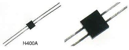
Photo 1 The first Hall element H-400A, production began in 1975
Hall Element H-400A is packaged by epoxy resin use of plastic case (named CASE-method):
-Vacuum deposition technology on mica substrates
-High-sensitivity process using a method of peeling off a thin film of InSb from the mica substrate and adhering it to a ferrite substrate
-Improving temperature dependency by constant voltage drive
-Connecting the Hall element and leads by soldering
But quality issue occurred about the thermal stability, leading to a complete review of the element design and manufacturing process for upcoming VTRs and FDDs. In 1983, they had overcome all the following challenges.
-Achieving the thermal stability required for automated mounting at 260°C, connecting the Hall element and leads bonded by Au-wire, and
Cu/Ni/Au three-layer electrode for Au-wired.
-Establishing mass production technology. From hand made to automated machine
Production of the newly designed HW Series (HW-300A, HW-101A, and HW-300B) began in June 1983.
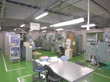
Photo 2 Asahi Kasei Electronics' Nobeoka Plant (Vacuum evaporation process)
Photo 3 Three types of thin film InSb Hall Elements (HW-101A(SMT), HW-300A(DIP), HW-300B(SIP) ), production began in June 1983.
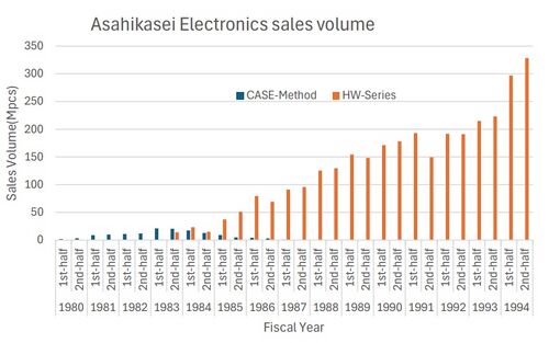
Figure 1 Sales volume of Hall element of Asahi kasei Electronics. ((Graph the data of Asahi Kasei Electronics The Biographical Sketch)
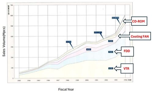
As shown in Figure 1, sales volume of the HW-series has grown rapidly since production began in 1983.The primary applications for Hall elements in the 1980s were VTRs and FDDs of PCs. Asahi Kasei's market share for Hall elements rapidly rose from 34% at the beginning of 1982 to 54% in 1987 and 60% in 1989. This shows how widely used the HW series Hall elements were. While they are no longer used in VTRs or FDDs today, their use has expanded to include cooling fans in air conditioners and servers, and motors for power tools. Approximately one billion units are still used each year, contributing to human society. The birth of the HW Hall elements in 1983 was an essential sensor for the development of the video, electrical, and information industries. It ushered in the era of personal video, where individuals could record and store videos, the widespread use of PCs, and the arrival of the information and communications era, including the Internet. It was the HW series Hall elements, born in 1983, that opened the door to this new society.
Figure 2 Annual sales volume of HW-series Hall elements by application. (From Asahi Kasei Electronics The Biographical Sketch)
Furthermore, the HW series has not only contributed to industry, but has also made significant contributions to advances in academic fields such as semiconductor thin-film magnetic sensor engineering, electronically controlled motor technology, electron transport in narrow bandgap compound semiconductors such as InSb, and quantum structures. Its achievements in changing the state of society and supporting the development of the global electronics and information industries, as well as academia and culture, are equivalent to an IEEE milestone. In 2014, it was recognized by the Institute of Electrical Engineers of Japan (IEEJ) as an electrical technology that has made a significant contribution to society.
Principles and Importance of Thin-Film InSb Hall Elements
Fundamental Principle of the Hall Effect
Hall effect was discovered as a magnet-electric phenomena in 1879 by Edwin H. Hall and named Hall effect later.
Hall effect produces a voltage or Hall voltage VH proportional to the magnetic field when current flows through a semiconductor under a perpendicular magnetic field.
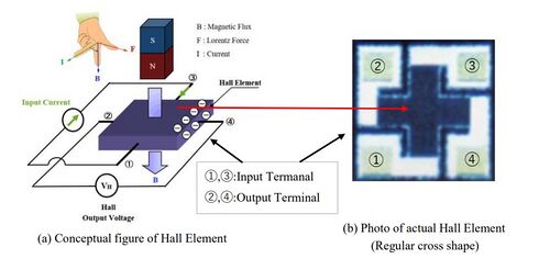
Next, expression of Hall voltage VH under 2 driving methods are shown. Hall element is a magnetic sensor used Hall effect made from semiconductor plate with 2 input electrodes (1,3) and 2 output electrodes (2,4).
Figure 3 (a)Hall element principal and Hall element with input electrodes 1, 3 and output electrodes 2,4.
Arrow means applied magnetic field with magnetic flux density B
(b)Photo of actual Hall element
Practically Hall elements are operated in either constant current or constant voltage modes. The temperature characteristics parameters vary depending on which method is used.
-Constant Current Drive: When a constant current (Ic) is applied to terminals 1 and 3, the output voltage VH at terminals 2 and 4 can be
expressed by the following equation:
VH = RH × (1 / d) × Ic × B ----- (1)
Here, RH is the Hall coefficient, and d is the thickness of the semiconductor film in the direction perpendicular to the terminal surface.
The Hall coefficient RH is defined using the electron charge e and the carrier concentration n as follows:
RH = 1 / (e × n) -----------------(2)
The temperature characteristic of the output voltage in constant current drive is determined by the temperature dependence of RH.
-Constant Voltage Drive:
When a constant voltage (Vc) is applied to terminals 1 and 3, the output voltage at terminals 2 and 4 can be expressed by the following
equation:
VH = μH × (W / L) × Vc × B ----(3)
Here, μH is the electron mobility, and W and L are the lengths in the directions of terminals 2-4 and 1-3, respectively. The temperature
characteristic of the output voltage VH in constant voltage drive is determined by the temperature dependence of μH.
Si and GaAs are common n-type semiconductor materials and have been used in electron devices, but their low electron mobility μH makes them unsuitable for magnetic sensors. On the other hand, InSb has high electron mobility, but has not been used in electron devices and is difficult to use in mass production. It also has poor temperature characteristics due to its narrow band gap.
The temperature coefficient of the Hall coefficient(RH) of the thin-film InSb deposited on mica substrate was measured as -2%/°C, while the temperature coefficient of electron mobility (μH) was measured as ±0.1 to 0.2%/°C, indicating that the temperature characteristics are significantly improved by constant voltage drive.
Thin-Film Advantages
Thin-film embodiments, especially submicron InSb layers, bring significant advantages
-Conventional bulk InSb has a low resistance of only a few ohms. On the other hand, thin-film InSb has a high resistance of several hundred ohms, allowing it to be used directly in electronic circuits. Furthermore, its high resistance enables constant-voltage drive and improves temperature characteristics:
Bulk InSb (constant current drive): -2%/°C → Thin-film InSb (constant voltage drive): ±0.1-0.2%/°C
-Thin-film InSb enables to adapt IC processes such as photolithography and etching etc, facilitating mass production and low costs.
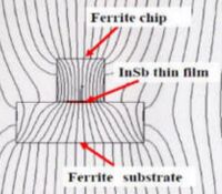
-Thin-film InSb makes it easy to create ferrite sandwich structure to increase sensitivity.
Figure 4 Ferrite sandwich structure of high-sensitivity InSb thin-film Hall element and collimation of magnetic flux at gap between ferrite magnetic chip and substrate :
Development and Commercialization
Research and Early Technological Breakthroughs
Asahi Kasei began dedicated R&D on thin-film InSb Hall elements in 1973.During the first two years, thin-film vacuum deposition, magnetic amplification structure, and temperature characteristics were investigated.
-Thin-film vacuum deposition: thin-film InSb on mica substrate by “two-temperature multi-boat method(2-boat)” achieved high electron mobility of -30,000 cm2/Vsec.
-Magnetic amplification structure: ferrite sandwich structure significantly increased sensitivity.
-Temperature characteristics: Constant voltage drive improved the temperature characteristics of Hall element.
were discovered.
Based on these results, samples of Hall element named “H-400” were available in 1975.The size of Hall element is 2.6mm square. In the next year, Asahi Kasei began production of a Hall element “H-400” for drive motors for record players.
In 1976, Hall elements with a smaller size to 1.7 x 1.8 mm were released and had improved costs and productivity. Rigorous reliability test (85°C, 85% RH, 500 hours) was passed in customer evaluation, confirming its high quality.
Manufacturing Scale-Up in 1980-1982
In 1980, Asahi Kasei restructured its operations for future expansion. “Miyazaki Electronics”, manufacturing subsidiary of Asahi Kasei, was established in Nobeoka City miyazaki prefecture, clarifying responsibilities with Asahi Kasei handling sales and Miyazaki Electronics handling manufacturing.
In July, mass-production vapor deposition machine for 4-boat was in operation. And mass production of thin-film InSb started at the end of the year. Smaller Hall element with 1.75mm square were released in next year to meet customer demand.
Meanwhile, quality problem such as heat stability was issued. As a countermeasure, the team began investigating the use of gold wire to connect the electrodes of Hall elements and leads. In 1982, the company adopted a three-layer electrode structure of Au/Ni/Cu for the Hall elements, ensuring a durable electrode structure compatible with gold wire.
At the end of 1982, Asahi Kasei restructured its operations again. “Miyazaki Electronics”, manufacturing subsidiary, was renamed Asahi Kasei Electronics. Asahi Kasei Electronics not only manufactured Hall elements but also sold Hall elements, establishing a structure that allowed it to take full responsibility for all aspects of Hall elements, from manufacturing to sales. Completely independent from the chemical company Asahi Kasei, it established a structure that enabled it to flexibly respond to markets and customers in the electronic components industry.
Commercialization Challenges in 1983
In January 1983, the structure and process for the Hall element (HW series) were finalized, significantly improving productivity and heat stability.
Major technological breakthroughs included further miniaturization of the Hall element (1.25 mm square), the adoption of a three-layer Au/Ni/Au electrode structure that could withstand gold wire connection, and plastic package (gold wire connection, formed by transfer molding) compatible with customers' automated mounting processes.
In June 1983, production of the HW-101A and HW-300A, which adopted this new process and structure, began, and the following month, production of the HW-300B, which had a different package, began. By September, 957kpcs Hall elements had been shipped. The sales of HW series products were remarkable, with 14.9 Mpcs shipped by March of the following year. These events are recorded in reference 1. An excerpt from the relevant section is shown in Photo 4.
Photo 4 (a)Chronology and (b) sales volume showing that production of the HW series Hall elements began in 1983 (from reference [1])
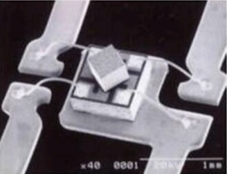
Photo 5 Inside HW-101A Hall element (Au-wire bonding)
Productivity of HW-series is remarkable, Sales volume reached 255 million in 1988, and all products sold by Asahi Kasei Electronics became the HW series. Thus, Asahi Kasei Electronics HW series became Hall elements that led the magnetic sensor market, unrivaled by competitors. What has driven this market growth since 1983 is the widespread adoption of HW series in brushless motors for VTR, FDD, CD/DVD-ROM. HW series Hall element captured over 70% of the global market, driven by broad adoption in brushless motors for electronics and appliances. By 2024, Asahi Kasei had produced over 40 billion HW series Hall elements, supporting supply chains worldwide.
Legacy and Continued Evolution
The thin-film Hall sensor’s legacy continues through its derivatives:
-Hybrid Hall effect IC
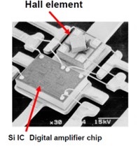
Hall effect ICs (Hall ICs) are magnetic sensors that combine a Hall element with a signal processing circuit. Output voltage of Hall elements is amplified and shaped by the signal processing circuit and output as a digital or analog signal. For customers, Hall ICs are easier to design than Hall elements.
Photo 6 Inside Hybrid Hall effect ICs (Au-wire bonding)
Social & Industrial Impact
In the late 1970s, Japanese electronics manufacturers focused their efforts on the development of personal audio equipment and home-use VCRs as the next big products after stereos and televisions. Information equipment makers were focusing their efforts on the development of consumer electronics products. The company focused on miniaturization of computers and development of personal computers. The key technology for all of these was an ultra-compact motor capable of high-precision rotation control.
The new motor that would solve these requirements was a motor without a contact switch, which is a source of electromagnetic noise, with a rotor that does not require a power supply, and with a high degree of angular velocity control. Thus, a brushless motor technology was desired that could be manufactured in a compact size without contact switches and with a drive circuit capable of precisely controlling rotation at the desired angular velocity. This is exactly what was required for the new power technology of electronically controlled motors. And an ultra-compact, high-sensitivity Hall element is a key device in these brushless motors.
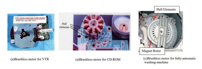
Photo 7 Brushless Motors for several applications
When motor technology changes, the systems that use it also change dramatically, giving rise to new technological systems. Hall elements transformed broadcast station VTRs into home videotapes, and huge computers gave rise to PCs that could be used exclusively by individuals. Hall elements made it possible to miniaturize PC memory (FDD, CD, DVD-ROM). In this way, changes in motor technology led to the development of many home appliances and had a huge impact on society. They made the final dream of the 20th century - videos, PCs, and the Internet - a reality. Then, in the 21st century, they were widely applied to cooling fans, and further development took place.
Why It Merits IEEE Milestone Recognition
-Hall elements were considered to have low sensitivity as magnetic sensors and were difficult to mass-produce in 1970-80s.
-Various innovations, including thin film, magnetic amplification, packaging etc made it possible to mass-produce high-performance Hall elements. As a result, Hall elements were widely used in VTRs, FDDs, and other devices in the 1980s, and they became widely recognized as a practical magnetic sensor. Since then, Hall element has come to be widely used to enhance the functionality of various electronic devices.
-A new market was created for brushless motors for home appliances using Hall elements.
This marks an important milestone in the history of magnetic sensing technology.
Conclusion
Asahi Kasei’s thin-film InSb Hall elements stand as a cornerstone of modern sensor technology. Their technical ingenuity, market penetration, and societal impact have been profound. By enabling the era of compact, electronically controlled motors and efficient systems, they have touched billions of lives. Granting IEEE Milestone status would aptly honor this deceptively simple yet transformative innovation.
What obstacles (technical, political, geographic) needed to be overcome?
Obstacles to Overcome
Technological Challenges
In the 1970s and early 1980s, the Asahi Kasei team faced four major technical hurdles:
- Industrial-scale vacuum deposition: Conventional thin-film InSb were low electron mobility(-5000cm²/V·s).
Solution: "two-temperature, multi-source vacuum evaporation method" was invented.
- Magnetic sensitivity shortfall: High-mobility films still lacked sufficient sensitivity.
Solution: Ferrite-sandwich structure was developed.
- Thermal drift control: InSb sensors suffered temperature coefficients of –2%/°C.
Solution: Combining thin-film high-resistance material with constant-voltage driving reduced drift to ±0.1–0.2%/°C.
- Sensor packaging: Bare chips with soldered lead had quality problem for automatic soldering.
Solution: Resin-molded packages with Au-wire were designed. It is capable of surviving SMT reflow at 260 °C, the first such implementation for compound-semiconductor sensors.
Each of these technical breakthroughs was essential for transitioning from lab prototypes to mass-producible components, enabling industrial scalability.
Organizational & Interdisciplinary Hurdles
Asahi Kasei, a chemical company, faced significant challenges when it entered the compound semiconductor industry.
Solution:
- A chemical company embracing semiconductor electronics required new expertise and organizational models.
- Chemists, and physicists collaborated intensively to bridge knowledge gaps.
- Many dismissed the project as academically biased. Credibility was built only after rollout of the HW Series that met rigorous industrial specs.
Infrastructure & Supply-Chain Barriers
Building a semiconductor-capable plant in rural Nobeoka posed logistical challenges.
Solutions:
- Facilities: Specialized vacuum chambers, cleanrooms, and advanced thermal control systems were designed from scratch.
- Human resources: Remote location necessitated relocating and training staff lacking semiconductor experience.
- Materials sourcing: Ultra-pure InSb were hard to buy—supply-chain development.
These infrastructure solutions ensured stable, high-quality production outside existing industrial hubs.
Market Adoption & Distribution
Entering a competitive component market required more than better sensors.
Solutions:
- Sales channels: Asahi Kasei created dedicated teams to engage motor manufacturers.
- Technical support: Design-in assistance became essential for adoption in brushless motors.
- Quality assurance: Strict process control and after-sales service.
These efforts accelerated the HW Series transition from lab success to global industrial deployment.
This multi-front strategy exemplifies the persistence, ingenuity, and systems thinking that characterize IEEE Milestone-level innovation.
What features set this work apart from similar achievements?
What Features Set This Work Apart from Similar Achievements?
In the 1970-1980s, Hall elements were primarily used in laboratories to measure magnetic fields. And they were handmade by polishing expensive InSb single crystals (high electron mobility), making low productivity and expensive, and did not have ferrite sandwich structure.
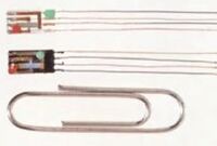
The other type of Hall elements was thin-film InSb Hall element, but it had very low sensitivity and was not plastic packaged, and it was difficult to use in mass production. That’s because the properties of the thin film InSb deposited on glass or ferrite substrates were poor, as a result, they could not go beyond the level of Sakai's paper [3]. And it was not a thin-film technology that could lead to a breakthrough in factory production technology as a semiconductor production process.
Photo 8 Typical thin film Hall Elements in 1970-1980s
On the other hand, the thin-film technology of Asahi Kasei was able to mass-produce high-performance thin films, and by the four breakthroughs previously described, it had become a factory production technology. In other words, they had made a breakthrough by improving thin-film technology to a production technology. This decided the outcome.
First Large-Scale Production of Thin-Film InSb:
Establishing mass-production technology for thin film InSb is the most crucial. Fabricating thin film InSb by vacuum deposition was a trial-and-error process.
-Selection of deposition substrate
Substrates such as ceramic, glass, and cleaved mica were tested. Thin mica substrates, with their heat resistance and atomically smooth surface, produced InSb thin films with the highest electron mobility. Furthermore, mica substrates were less expensive than other substrates.
-Extra-large vapor pressure difference between In and Sb and overcoming it
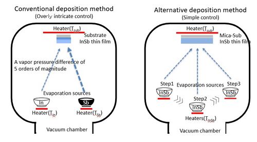
The ideal stoichiometric composition of InSb thin films is In:Sb=1:1, but the vapor pressure of Sb is approximately 10,000 times that of In, five-order difference. This was a major obstacle to fabricating thin InSb films by vacuum evaporation. The standard deposition method at the time was developed by Günter in Germany, in which In and Sb were placed in separate evaporation sources with a distance and the vapor pressure of the In and Sb was controlled by adjusting their temperature (Tin and Tsb and substrate Tsub.) to produce InSb thin films with a 1:1 composition. This method, known as the "three-temperature method (Tin-Tsb-Tsub)", involves controlling the different temperatures of In (Tin), Sb (Tsb), and the substrate (Tsub) during vacuum deposition. Sb was evaporated by sublimation, therefore the incident angle of the In and Sb vapors on the substrate surface are different. Therefore, thin films with 1:1 composition can only be produced on a small area on the substrate center, making large-area production difficult. Thus, producing large-area InSb thin films is extremely difficult. Furthermore, at the time to obtain films with good crystallinity, the substrate must be uniformly heated to approximately 400°C. This heating is performed at a temperature slightly below the melting point of InSb, which is deeply involved in the crystal growth of the InSb thin film. Therefore, substrate heating during evaporation is also a major problem.
- Investigation of new vapor deposition methods
In the mid-1970s, despite many challenges, the team developed an industrial vapor deposition method capable of depositing multiple films at once. They investigated a vapor deposition method using single crystal InSb as the evaporation source, including the design and construction of the equipment, which ensured that the angle of incidence of In and Sb vapors on the substrate surface was the same for each substrate, even when multiple substrates were loaded into the evaporation machine. Over two years of experiments, the team discovered that dividing high-purity single-crystal InSb into multiple evaporation sources and sequentially heating the sources to evaporate InSb resulted in higher electron mobility than previous evaporation methods. This result was important: while a five-digit vapor pressure difference caused Sb-rich and In-rich vapors to alternately reach the substrate, moreover, the same amount of In and Sb reaches the substrate. And substrate heating caused diffusion of In and Sb within the film, suppressing gradient alloying, resulting in a stoichiometric 1:1 In:Sb composition, resulting in a thin film with high electron mobility. Therefore, the team constructed the new evaporation machine with multiple evaporation sources and continued to explore crystal growth conditions that would yield high electron mobility. As a result, we discovered a new deposition method, the "two-temperature multi-source vacuum evaporation method(Tinsb-Tsub)" which involves sequential heating, and adjusting the temperature of the deposition source for sequentially evaporating InSb(Tinsb) and the substrate heating temperature(Tsub). This method established new technology for mass-producing high-quality InSb thin films with a 1:1 composition on large areas (36sheets,2-inch square substrates).
Figure 5 Comparison of the concept of vacuum deposition methods, (a) three-temperature method, (b) "two-temperature multi-source vacuum deposition method
The resulting thin films had a thickness of 0.8 μm, a sheet resistance of 150 Ω, and an electron mobility of 20,000–30,000 cm2/Vs, making them suitable for the fabrication of highly sensitive Hall elements. The electron mobility of InSb thin films on mica was approximately 5,000 cm2/Vs in conventional "three temperature method". Using this thin film, it became possible to fabricate highly sensitive Hall elements with magnetic field detection sensitivity four to six times higher than conventional methods. This was a major breakthrough in thin-film material fabrication and established the fundamental technology for materials fabrication. The ability to mass-produce thin films with excellent characteristics even on large areas significantly contributed to the subsequent mass production of Hall elements.
Magnetic Amplification Structure Using Soft Ferrite:
High-mobility films still lacked sufficient sensitivity. It was known that sensitivity could be increased by using a magnetic amplification structure, but it was thought that this structure would be impossible to apply to mass production. A common magnetic amplification structure would involve vapor-depositing an inorganic insulating film on ferrite and then vapor-depositing InSb, but it is difficult to form a high-quality InSb thin film on that substrate. On the other hand, high-quality InSb thin films can be formed on mica, but mica is fragile, and it was thought that this would be impossible to use substrate of Hall elements in mass production. Asahi Kasei devised a method to transfer the InSb thin film on mica to ferrite substrate with an adhesive and applied this to the magnetic amplification structure. This method enabled highly sensitive Hall elements, achieving practical sensitivity.
Temperature Stability Through Thin-Film Engineering:
One longstanding issue with InSb Hall sensors was their high temperature coefficient of Hall voltage VH, i.e. sensitivity.
Generally, temperature characteristics are improved by impurity doping to InSb. However, doping reduces sensitivity, making it unusable for practical use. Meanwhile, Asahi Kasei discovered that changing the driving method of the Hall element from the conventional constant current to a constant voltage. Thin-film approach, coupled with high input resistance design and constant-voltage drive methodology, reduced the temperature coefficient of the Hall voltage from −2%/°C (typical of conventional devices) to an unprecedented ±0.1–0.2%/°C
Packaging and Integration with Modern Manufacturing Processes:
Recognizing that sensor performance alone was insufficient for adoption, a compact, plastic-package that was compatible with automatic mounting process were designed. To improve heat stability, the team considered using Au wire to connect the Hall element electrodes and leads instead of soldering. To achieve Au-wire connection, the Hall element electrodes needed to be significantly strengthened, and a new electrode consisting of a three-layer thin film of Au/Ni/Cu was developed. This electrode technology made it possible to connect Au wire to InSb thin film with soft adhesive under layer on the ferrite substrate. This patented electrode technology enabled mass production of the HW series Hall elements and achieved excellent heat stability up to 260°C.
Figure 6 (a)H-400A connected by solder, (b)HW-101A connected by Au wire ,260℃ heat resistive package. (c) Photo of Au wired HW-101A Hall element.
This made it possible to integrate the Hall sensor into printed circuit boards in a fully automated fashion, reducing assembly costs and improving reliability. This packaging strategy enabled the device to be used widely in high-volume manufacturing process, including VTRs, PC.
In summary, while many researchers in the 1970s and early 1980s explored thin film Hall technologies, Asahi Kase’s work stands out for having crossed the crucial threshold from lab-scale experimentation to industrial production and widespread adoption. This work was not just about improving sensitivity; it was about delivering a solution that met the full demands of the electronics industry: high performance, mass manufacturability, environmental robustness into emerging technologies. The InSb thin film Hall element represents a landmark achievement in the history of semiconductor sensors, enabling the rise of intelligent motion control in modern electronics and leaving an enduring legacy in both technology and industry.
Why was the achievement successful and impactful?
Why was the achievement successful and impactful?
In the 1970s, InSb Hall elements were thought to be impractical as magnetic sensors (they could only be used to measure magnetic fields), but through various improvements and breakthrough, HW-series Hall elements, they were widely applied to consumer devices such as VTRs and PCs, making thin-film Hall elements widely known as practical magnetic sensors. This is a reason why thin film Hall element was successful and impactful.
What set Shibasaki’s Hall element apart was not just its high sensitivity, but the holistic approach taken to address the full spectrum of applications such as various electrical devices.
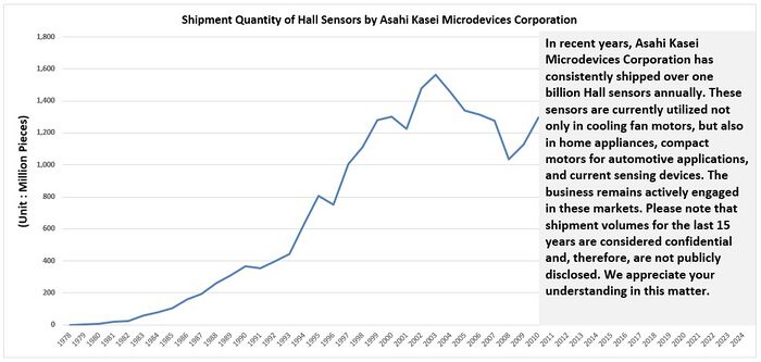
Production of the HW series Hall elements began in 1983, toward the end of the 20th century. Their applications expanded, first as magnetic sensors for small DC motors in VTRs and FDDs, then CD/DVD-ROMs, leading to a rapid increase in production volume. They were also used as cooling fans in PCs, air conditioners, and servers, contributing to the expansion and energy conservation of these devices. In recent years, their use as drive motors for power tools such as electric screwdrivers have contributed to their miniaturization and battery-powered operation, further expanding their applications. Even today, HW series Hall elements are steadily produced at a rate of 1 billion units per year. Of the three HW series models first produced in 1983, the HW-101A and HW-300B are still produced using the same production process, demonstrating their high level of technological sophistication and ability to meet customer needs. As mentioned above, thin-film Hall elements are magnetic sensors that have realized the human dream of a richer life. This is evidenced by the production volume and the photographs of application devices in Photo 7 and Figure 7.
Figure 7 Shipment quantity of Hall sensors by Asahi Kasei Microdevices Corporation. (Asahi Kasei Electronics was consolidated into Asahi Kasei Micro Devices Corporation)
Supporting texts and citations to establish the dates, location, and importance of the achievement: Minimum of five (5), but as many as needed to support the milestone, such as patents, contemporary newspaper articles, journal articles, or chapters in scholarly books. 'Scholarly' is defined as peer-reviewed, with references, and published. You must supply the texts or excerpts themselves, not just the references. At least one of the references must be from a scholarly book or journal article. All supporting materials must be in English, or accompanied by an English translation.
Bibliography
[1] Asahi Kasei Electronics The Biographical Sketch, September 1995
US Translated:Media:Ref1_e.pdf
[Remarks] This book was published in 1995 to commemorate the 15th anniversary of the founding of Miyazaki Electronics (the predecessor of Asahi Kasei Electronics) in 1980. It chronologically summarizes the history of development, production, and sales from the start of Hall element development in 1973 to 1995. It also states that the thin-film Hall element (HW series) was shipped in the first half of 1983.
[2] I. Shibasaki, "High sensitivity InSb Hall elements and their development for practical use", Monthly Report J. Chemical Industry Association, vol41, May 1988
US Translated: Media:Ref2_e.pdf
[Remarks]This paper summarizes the history of thin film Hall elements at Asahi Kasei and technological development about 3 breakthroughs including “driving methods”, “magnetic amplification structures”, and “packaging”. It also reported manufacturing process.
[3] I. Shibasaki, "Vapor-deposited Hall element and its characteristics", Integration of advanced semiconductor technology, Management Systems Research, pp.373-389 Chapter3 section11,1980
US Translated: Media:Ref3_e.pdf
[Remarks]This paper summarizes the technological development of thin-film Hall elements about 3 breakthroughs including “driving methods”, “magnetic amplification structures (detail)”, “vacuum deposition (compared to conventional technology)”. Asahi Kasei's thin film InSb fabrication technology. Thin film InSb with electron mobility of 20,000 to 30,000 cm2/V・sec was obtained by two-temperature multi-boat deposition method, and the measurement results of its magnetic and electrical properties, and magnetic amplification structure increases the sensitivity by three times, had been reported.
[4] Yoshio Sakai and Masahide Osita , “Preparation of InSb film and measurement of Hall Characteristics”, IEEJ Journal of Industry Applications, Vol.80, pp.36-41,1960
US Translated: Media:Ref4_e.pdf
[Remarks] Thin film InSb fabrication technology by vacuum deposition from around 1960 to 1980. It has been reported that the electron mobility of InSb thin film on mica was 4840 cm2/v・sec.
[5] I. Shibasaki, "High-Sensitivity InSb Thin-Film Hall Elements with Ferrite Sandwich Structure and Their Extensive Commercial Application(Invited paper)", J. Jpn. Soc. Powder Metallurgy Vbl. 61 Supplement, No. SI, PP. S335-S339, March 2014
[Remarks]This paper summarizes the technological development of thin-film Hall elements about 2 breakthroughs including “driving methods”, “magnetic amplification structures”. It also reported the expansion of thin film Hall element applications and sales volume by application.
[6] I.Shibasaki, "High Sensitive Hall Elements by vacuum deposition", Technical Digest of 8th Sensor symposium, pp.211-214,1989
[Remarks] This paper summarizes the technological development of thin-film Hall elements about 2 breakthroughs including “driving methods”, “magnetic amplification structures”.
[7] I.Shibasaki, "The practical Hall Elements as magnetic sensors by thin film technology (Invited paper)", IEEE Lasers and Electro Optical Society,1995
[Remarks] A review of vacuum-deposited thin-film InSb Hall elements.
[8] I. Shibasaki,"InSb and InAs Hall Elements from Asahi Chemical", Compound Semiconductor, September/October,1996 Media:R17.pdf
[Remarks] This magazine article summarizes the recent expansion of applications and quantities of thin-film InSb Hall elements, and Asahi Kasei's share of the global market for Hall elements had reached 70%. It also reported on the next-generation Hall element, the InAs Hall element.
[9]I. Shibasaki,"Physical properties of InSb single crystal thin films and their application to magnetic sensors", Transactions of the Institute of Electrical Engineers of Japan,2003
US Translated: Media:Ref9_e.pdf
[Remarks] This paper summarizes the recent expansion of applications and quantities of thin-film InSb Hall elements, and the raw material and energy saving effects of brushless motors using Hall elements.
[10] I.Shibasaki, "Recent Advances in thin film magnetic sensors and development applications”, Journal of Advanced Science vol.17 No3&4,2005
US Translated:Media:Ref10_e.pdf
[Remarks]This article summarizes the development of applications for thin film InSb Hall elements.
[11] K.Ishibashi, I.Okada, I.Shibasaki, "High Sensitive Hall Effect ICs with Thin film Hall Elements", Sensors and Materials vol14 No.5 pp.253-261,2002
[Remarks]This paper summarizes the hybrid Hall ICs, which combine HW-series Hall element and a processing circuit in a single package.
Patents
[P1] Patent related to Thin film Hall Element of Ferrite Sandwich Magnetic Amplification structure and manufacturing method of this Hall element, December 12. 1973, (JP)Tokko No.51-45234,
Media:JPB 1976045234.pdf,
US transrated: Media:US Trans 1976045234.pdf
[Abstract]
Thin film Hall Element of Ferrite Sandwich Magnetic Amplification structure and manufacturing method of this Hall element
[P2] Patent related to Manufacturing method of ferrite sandwich thin film Hall Element, April 28,1975(JP)Tokko No.53-46675,
Media:JPB 1978046675.pdf,
US transrated: Media:US Trans 1978046675.pdf
[Abstract]
Manufacturing method of ferrite sandwich thin film Hall element formed on a magnetic substrate overlaying an organic insulating layer with a step of forming a thin film by vapor deposition and mechanically peeling the magnetic material and adhering a second magnetic material on a magnetic substrate.
[P3] Patent related to the structure of mold Hall element, May 10,1985. (JP)TokkoNo4-62474
Media:JPB 1992062474.pdf ,
US Pat.4908685: Media:USA1004908685.pdf
[P4] Patent related to Manufacturing method of mold Hall element, May 10,1985. (JP)TokkoNo4-62475
Media:JPB 1992062475.pdf ,
US Pat.4908685: Media:USA1004908685.pdf
[Abstract]
A magnetoelectoric transducer complying a group Ⅲ-Ⅴ compound semiconductor thin film formed as a magnetic field sensing portion on a substrate overlaying an organic insulating layer and a multilayer wirebonding electrode. And a bonding wire is connected directly to the wirebonding electrode.
Awards
[A1] Ōkouchi Memorial Production Prize,1987
Media:A1 Ōkōchi Prize 1987 2.pdf
[Remarks]
-Development and Mass Production of High-Sensitivity InSb Hall Elements
-Awarding Organization: Ōkochi Memorial Foundation
-Recipient: Asahi Chemical Industry Co., Ltd.
-Citation: Asahi Chemical Industry Co., Ltd.'s high-sensitivity InSb thin-film Hall element of the HW series, which is based on the vacuum deposition method, was the first in the world to have an annual production volume of more than 150 million units, and its excellent mass production technology was awarded.
-Purpose: The Ōkouchi Memorial Production Prize was established to honor individuals or organizations that have made significant contributions to the field of production engineering and industrial technology, aiming to promote the advancement of Japan’s industrial capabilities.
-Value of the Prize: It is one of Japan’s most prestigious awards in the field of industrial technology. Receiving this prize signifies high recognition of technological excellence and innovation.
[A2] Invention Encouragement Award,1992,
Media:A2_Invention Encouragement Award 1992 2.pdf
[Remarks]
-Awarding Organization: Japan Institute of Invention and Innovation (JIII)
-Recipients: Ichiro Shibasaki, Kohei Nonaka, Tsuyoshi Shimizu, (Asahi Chemical Industry Co., Ltd.)
-Citation: Patent award for [P2] patent
-Purpose: Contribute to scientific and technological advancement. Encourage inventive and creative activities.
-Value of the Award: Established in 1921, the Regional Commendation for Invention aims to promote local industry and encourage technological innovation across Japan’s regions.
[A3] Invention Encouragement Award,1999,
Media:A3_Invention Encouragement Award 1999.pdf
[Remarks]
-Recipients: Ichiro Shibasaki , Takashi Kajino,(Asahi Chemical Industry Co., Ltd.)
-Citation: Patent award for [P3] patent
Others are the same as [A3]
[A4]The foundation of electricity 2013,
Media:A4_The foundation of electricity.pdf
[Remarks]
-Awarding Organization: The Institute of Electrical Engineers of Japan (IEEJ)
-Recipient: Asahi Kasei Corporation
-Citation: Asahi Kasei was awarded for its development and commercialization of Thin-Film Indium Antimonide (InSb) Hall Elements in 1983. This innovation revolutionized magnetic sensing technology, enabling the widespread adoption of brushless DC motors and laying the foundation for electronic control in consumer electronics, computing .
-Purpose: The "One Step on Electro-Technology" honors the achievements of electrical technology that have made a great contribution to social life, and the achievements of electrical technology that has either historical technical value, social value, or academic and educational value for more than 25 years with the aim of widely disseminating its value to the world, making many people aware of the wonders and interests of electrical technology, and contributing to the development of electrical technology in the future.
-Value of the Award: The award signifies official recognition by a global technical organization of a This award is given to achievements with technical and social impact that can be recognized as milestones in electrical technology by the Institute of Electrical Engineers of Japan, that is an official recognition by Japan's leading academic organizations.
[A5] The Yamazaki-Teiichi Prise 2018,
Media:A5 The Yamazaki-Teiichi Prise 2018.pdf
[Remarks]
-Recipient: Ichiro Shibasaki, (Asahi Kasei Corporation)
-Presenter: The Foundation for Promotion of Material Science and Technology of Japan (MST Foundation)
-Award Category: Semiconductor and Semiconductor Devices
-Citation: Ichiro Shibasaki was awarded for his pioneering work in the development and commercialization of high-sensitivity thin-film Hall sensors using III-V compound semiconductors such as InSb and InAs. His innovations included: Fabrication of monocrystalline and polycrystalline thin films and quantum wells. Mass production of ultra-thin, high-sensitivity Hall elements.
-Practical applications in VCRs, PC cooling fans, HDDs, CD-ROMs, air conditioners, contactless current sensors.
-These sensors achieved 20–30 times higher magnetic sensitivity and significantly reduced temperature dependence, leading to cumulative production exceeding 30 billion units.
-Purpose of the Award: The Yamazaki-Teiichi Prize honors individuals who have made outstanding contributions to the advancement of science and technology in Japan, particularly in the fields of materials, semiconductors, and devices. It aims to promote innovation and recognize achievements that have had a significant impact on industry and society. This award commemorates Dr. Teiichi Yamazaki’s legacy and encourages pioneering research and development that leads to practical applications and industrial progress.
-Value of the Award: The Yamazaki-Teiichi Prize is one of Japan’s most prestigious honors in applied science and engineering. It signifies national recognition of technological excellence and societal impact. The award enhances the visibility of the recipient’s work and promotes further innovation in the field. Winning this prize places the recipient among Japan’s top innovators and validates the long-term industrial and academic significance of their contribution.
Supporting materials (supported formats: GIF, JPEG, PNG, PDF, DOC): All supporting materials must be in English, or if not in English, accompanied by an English translation. You must supply the texts or excerpts themselves, not just the references. For documents that are copyright-encumbered, or which you do not have rights to post, email the documents themselves to ieee-history@ieee.org. Please see the Milestone Program Guidelines for more information. Please email a jpeg or PDF a letter in English, or with English translation, from the site owner(s) giving permission to place IEEE milestone plaque on the property, and a letter (or forwarded email) from the appropriate Section Chair supporting the Milestone application to ieee-history@ieee.org with the subject line "Attention: Milestone Administrator." Note that there are multiple texts of the letter depending on whether an IEEE organizational unit other than the section will be paying for the plaque(s). Please recommend reviewers by emailing their names and email addresses to ieee-history@ieee.org. Please include the docket number and brief title of your proposal in the subject line of all emails.
