Milestone-Proposal:THE FIRST DEMONSTRATION OF THE SEMICONDUCTOR QUANTUM-WELL LASER DIODE, 1977
To see comments, or add a comment to this discussion, click here.
Docket #:2022-07
This proposal has been submitted for review.
To the proposer’s knowledge, is this achievement subject to litigation? No
Is the achievement you are proposing more than 25 years old? Yes
Is the achievement you are proposing within IEEE’s designated fields as defined by IEEE Bylaw I-104.11, namely: Engineering, Computer Sciences and Information Technology, Physical Sciences, Biological and Medical Sciences, Mathematics, Technical Communications, Education, Management, and Law and Policy. Yes
Did the achievement provide a meaningful benefit for humanity? Yes
Was it of at least regional importance? Yes
Has an IEEE Organizational Unit agreed to pay for the milestone plaque(s)? Yes
Has the IEEE Section(s) in which the plaque(s) will be located agreed to arrange the dedication ceremony? Yes
Has the IEEE Section in which the milestone is located agreed to take responsibility for the plaque after it is dedicated? Yes
Has the owner of the site agreed to have it designated as an IEEE Milestone? Yes
Year or range of years in which the achievement occurred:
1977
Title of the proposed milestone:
THE FIRST DEMONSTRATION OF THE SEMICONDUCTOR QUANTUM-WELL LASER DIODE, 1977
Plaque citation summarizing the achievement and its significance; if personal name(s) are included, such name(s) must follow the achievement itself in the citation wording: Text absolutely limited by plaque dimensions to 70 words; 60 is preferable for aesthetic reasons.
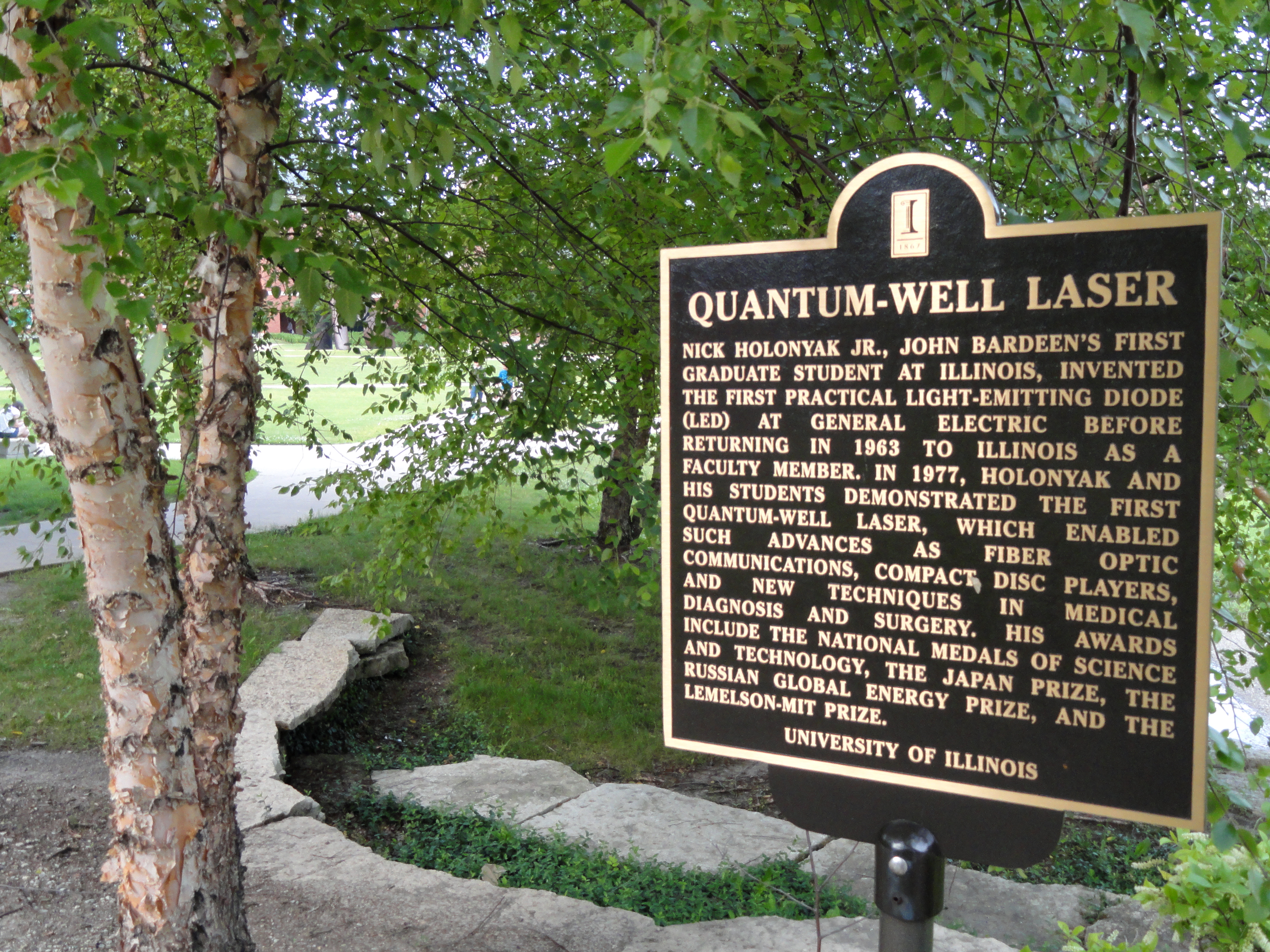
Semiconductor Quantum-Well Laser Diode, 1977 The first quantum-well laser diode was demonstrated in 1977 by Professor Nick Holonyak, Jr. and his graduate students in the Electrical Engineering Research Laboratory on the UIUC Campus. This was the first semiconductor diode laser to employ the “quantum-size effects” inherent in the physical and optical properties of ultrathin semiconductor layers in the active region of the device. Currently, billions of semiconductor quantum-well laser diodes and LEDs are manufactured every year.
200-250 word abstract describing the significance of the technical achievement being proposed, the person(s) involved, historical context, humanitarian and social impact, as well as any possible controversies the advocate might need to review.
IEEE technical societies and technical councils within whose fields of interest the Milestone proposal resides.
In what IEEE section(s) does it reside?
Region 4, Central Illinois Section
IEEE Organizational Unit(s) which have agreed to sponsor the Milestone:
IEEE Organizational Unit(s) paying for milestone plaque(s):
Unit: IEEE Photonics Society
Senior Officer Name: Rene Essiambre
IEEE Organizational Unit(s) arranging the dedication ceremony:
Unit: IEEE Central Illinois Section
Senior Officer Name: Jack Marck
IEEE section(s) monitoring the plaque(s):
IEEE Section: IEEE Central Illinois Section
IEEE Section Chair name: Jack Marck
Milestone proposer(s):
Proposer name: Russell D. Dupuis
Proposer email: Proposer's email masked to public
Please note: your email address and contact information will be masked on the website for privacy reasons. Only IEEE History Center Staff will be able to view the email address.
Street address(es) and GPS coordinates in decimal form of the intended milestone plaque site(s):
208 North Wright Street Urbana IL 61801 USA/40.114N; 88.228W
Describe briefly the intended site(s) of the milestone plaque(s). The intended site(s) must have a direct connection with the achievement (e.g. where developed, invented, tested, demonstrated, installed, or operated, etc.). A museum where a device or example of the technology is displayed, or the university where the inventor studied, are not, in themselves, sufficient connection for a milestone plaque.
Please give the details of the mounting, i.e. on the outside of the building, in the ground floor entrance hall, on a plinth on the grounds, etc. If visitors to the plaque site will need to go through security, or make an appointment, please give the contact information visitors will need. Nick Holonyak, Jr. Micro and Nanotechnology Laboratory on UIUC campus where semiconductor related research is carried out.
Are the original buildings extant?
No
Details of the plaque mounting:
Outside the building on the external facade near the entrance
How is the site protected/secured, and in what ways is it accessible to the public?
The site is on campus and is always accessible to the public.
Who is the present owner of the site(s)?
University of Illinois at Urbana-Champaign, Urbana IL 61801
What is the historical significance of the work (its technological, scientific, or social importance)? If personal names are included in citation, include detailed support at the end of this section preceded by "Justification for Inclusion of Name(s)". (see section 6 of Milestone Guidelines)
Historical Technological and Scientific Significance:
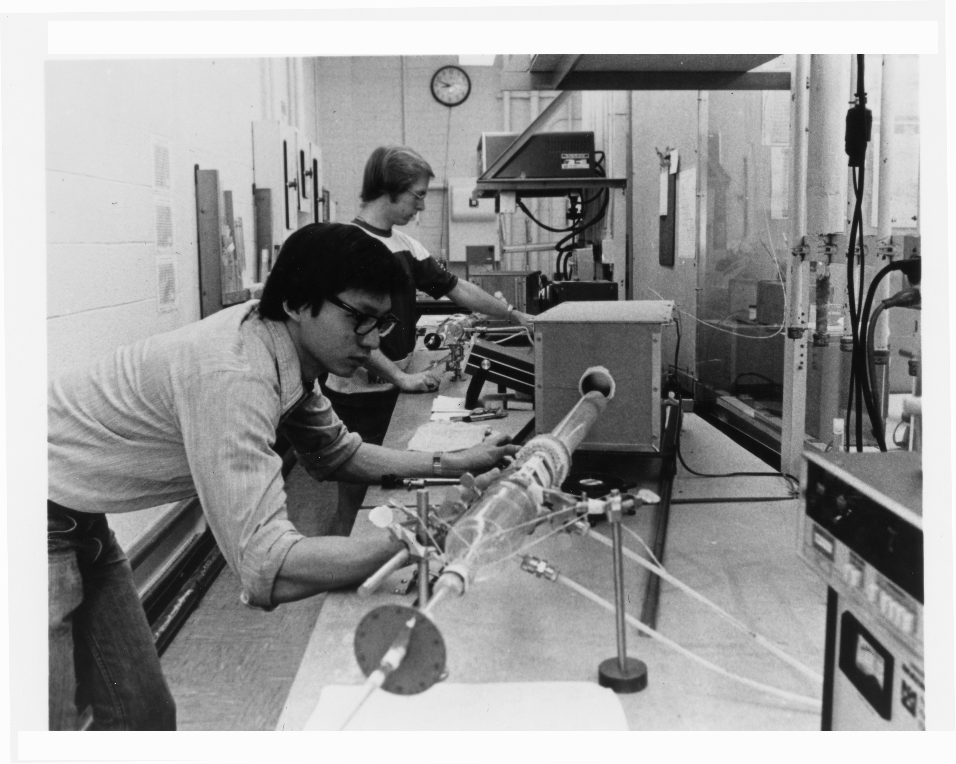
Holonyak, et al.’s demonstration of the first quantum-well laser diode (QW LD) in 1977 grown by liquid-phase epitaxy (LPE) [1] was a great surprise to almost everyone in the field of semiconductor lasers world-wide and was an important milestone achievement in this commercially important technological area. This work, and Holonyak’s very productive subsequent research on quantum-well lasers,[2] led to the further development of these concepts and to the commercialization of high-performance quantum-well-based semiconductor lasers [3] and light-emitting diodes that are universally used as compact coherent optical sources today for virtually all applications, including high-speed telecommunications, lighting, sensing, medical treatments, manufacturing, LIDAR, etc.
The theoretical electron transport properties of ultrathin heterostructures were first studied by R. Tsu and L. Esaki from IBM and reported in 1970.[4] This theoretical work focused on the tunneling of electrons through a ”finite superlattice”—multiple alternating thin layers of lattice-matched AlxGa1-xAs and GaAs. The optical properties of these heterostructures were not discussed in this early work—the focus was on the electrical I-V characteristics to demonstrate “tunneling effects”. The first epitaxial growth of such “superlattices” composed of ultra-thin III-V compound semiconductor heterostructures were reported by L. L. Chang, et al., at IBM in 1973. These superlattices were grown by a unique custom-made and very expensive computer-controlled molecular beam epitaxy (MBE) machine.[5] The properties of these AlGaAs-GaAs superlattices were studied using Raman spectroscopy and electrical I-V measurements. No photoluminescence properties were reported.
The first studies of the optical emission properties of ultra-thin semiconductor heterostructures were conducted by Dingle, et al., from Bell Labs in 1974.[6] These studies focused only on the low-temperature (~2K) photoluminescence of the optical properties of lattice-matched AlGaAs-GaAs heterostructures containing thin (~14-21nm) GaAs layers grown at Bell Labs by MBE. No devices containing such multiple-thin-layer active regions were reported. In 1975, J. P. van der Ziel, et al., from Bell Labs reported the low-temperature (15K) laser operation of optically pumped AlGaAs-GaAs multilayer heterostructures containing 50 GaAs “ultra-thin” layers ~8nm thick grown by MBE.[7] The optical pumping used a high-power optical parametric oscillator with 100ns pulses and corresponded to an equivalent current density estimated to be up to ~120kA/cm2. The pulsed optically pumped laser thresholds were estimated to be 15-36 kA/cm2. In 1976, R. C. Miller, et al., from Bell Labs reported a comparison of the optically pumped laser thresholds (again using an optical parametric amplifier pumping source) and quantum efficiencies for multilayer GaAs-AlxGa1-xAs heterostructures having 25-50 layer pairs of thin multilayer heterostructures [GaAs (8nm) - AlxGa1-xAs (24nm)] grown by MBE and conventional GaAs-AlxGa1-xAs double heterostructures grown by both MBE and LPE.[8] They reported the optically pumped thin multi-layer heterostructures exhibited 300K equivalent pulsed threshold current densities of 23-323 kA/cm2. The authors reported in a summary of the somewhat disappointing results of their optical pumping studies that “the lasing thresholds and quantum efficiencies of the multilayer units are far inferior to those of conventional MBE double-heterostructure lasers” and furthermore that “LPE double-heterostructure lasers are about a factor of 2 better with regard to thresholds and differential quantum efficiencies than their MBE twins.” So as late as June 1976, the Bell Labs reports of optical properties of multiple thin-layer “quantum-well” heterostructures were not promising and no MBE-grown “quantum-well” active region laser diode or even LED was reported prior to Holonyak’s LPE QW LD results reported one year later in June 1977. It was clear from this work at IBM and Bell Labs that even very expensive MBE machines were not capable of making high-performance quantum-well laser diodes—even in the “simple” GaAs-AlxGa1-xAs lattice-matched alloy system. The pulsed optically pumped laser thresholds at 15K reported by Bell Labs were quite high in comparison with the In1-xGaxP1-zAsz-InP LPE QW LDs reported by Holonyak, et al., that exhibited 77K laser operation thresholds as low as 890A/cm2 with pulsed current excitation. In fact, the first reported MBE-grown electrically pumped GaAs-AlxGa1-xAs system QW LDs were operated pulsed at 300K and exhibited thresholds ~2kA/cm2 and were not realized until November 1979 by Tsang, et al., at Bell Labs,[9] more than two years after Holonyak, et al.’s first In1-xGaxP1-zAsz quaternary QW LD report.
The early quantum-well laser results of Holonyak, et al., were surprising in that their QW laser diode device structures were grown using a “cheap” “low-tech” LPE system at a small university laboratory when the biggest, best financed, and most famous industrial semiconductor research labs and diode laser groups at IBM Research and Bell Labs Research were not able to make such devices by MBE or indeed, by any process. Both IBM and Bell Labs had extensive LPE laser diode materials and laser diode device technologies—yet they did not report any QW electroluminescent devices of any kind. However, the QW laser diode results from Holonyak’s group were even more astounding due to the fact that the quantum wells were composed of In1-xGaxP1-zAsz quaternary layers with InP barriers—not an inherently lattice-matched system with “simple” GaAs quantum wells–and much more complicated to grow than GaAs-AlxGa1-xAs!!! Today, virtually all commercial III-V compound semiconductor injection laser diodes (even vertical-cavity surface-emitting lasers-VCSELs and LEDs) are grown with quantum-well active regions. For example, the optical back bone of the Internet runs on quantum-well laser diodes, as does high-efficiency laser welding systems, face recognition (e.g., “Face ID” from Apple), optical sensors for computer mice, and other optical sensing systems, and sources for compact LIDAR systems and all high-performance LEDs.[10],[11] This innovation and demonstration has changed how the world creates and uses efficient light sources. The fact that Holonyak, et al., demonstrated this advance using a complex semiconductor quaternary epitaxial layer structure grown by a low-cost LPE process further makes this achievement exceptionally noteworthy in the history of technology and science and an example of what a motivated team with good ideas can accomplish.
References Uploaded: [1] E. A. Rezek, et al., Appl. Phys. Lett. 31, 288 (1977). E. A. Rezek, et al., IEEE Trans. Electron. Dev., ED-24, 1204 (1977). [2] According to an Engineering Village website search, N. Holonyak, Jr. has authored or co-authored over 396 reviewed technical journal papers on “quantum-well lasers” and related device properties in the period 1977-2012. Search performed 09-01-2022. [3] For example, Spectra Diode Labs (SDL) commercialized the high-power QW LD in an SBIR Granted in 1994 by BMDO to SDL for quantum-well laser diode production. [4] L. Esaki and R. Tsu IBM J. Res. Dev. 14, 61 (1970). [5] L. L. Chang, et al., J. Vac. Sci. Technol. 10, 11 (1973). [6] R. Dingle, et al., Phys. Rev. Lett. 33, 827 (1974). [7] J. P. van der Ziel, Appl. Phys. Lett. 26, 463 (1975). [8] R. C. Miller, et al., J. Appl. Phys. 47, 4509 (1976). [9] W. T. Tsang, et al., Appl. Phys. Lett. 35, 673 (1979). [10] https://www.globenewswire.com/news-release/2022/06/14/2462478/0/en/Laser-Diode-Market-is-estimated-to-Develop-at-a-CAGR-of-11-6-during-the-Forecast-Period-Observes-TMR-Study.html, accessed 08-29-2022. [11] https://www.yahoo.com/now/led-lighting-market-research-report-135900013.html, accessed 08-30-2022.
What obstacles (technical, political, geographic) needed to be overcome?
Holonyak had no access to advanced epitaxial semiconductor growth technologies e.g. molecular-beam epitaxy (MBE) that cost several hundred thousand dollars to purchase and were expensive to operate so he and his students created a unique form of simple liquid-phase epitaxy to grow these complex thin-layer heterostructures. Furthermore, these materials were quaternary III-V compounds containing four elements. These results were totally unexpected since researchers at Bell Telephone Laboratories and IBM Laboratories had not been able to demonstrate such devices despite having worked on the growth of thin-layer III-V heterostructures in the relatively simple AlxGa1-xAs-GaAs system using the most advanced and expensive MBE systems for many years prior to 1977.
What features set this work apart from similar achievements?
Holonyak's LPE-grown semiconductor quantum-well laser diodes were the first demonstrated diode lasers that employed ultra-thin "quantum-well" layers in the active region. In fact, Holonyak was the first to use the term "quantum-well laser" and "multiple quantum-well laser", terms now commonly used for these types of laser diodes. Until Holonyak's work, the only published results for lasers with "multiple thin active layers" were OPTICALLY PUMPED--not in a p-n junction diode form--and were grown by MBE and mostly operated at low temperatures 4-15K. Such demonstrations did not result in any practical devices being demonstrated. In fact, the first QW laser diodes grown by MBE were made at Bell Labs Murray Hill NJ by W. T. Tsang, et al., and published in Appl. Phys. Lett. 35 (9) 1 Nov. 1979 (manuscript received 6 July 1979). So it was essentially TWO YEARS AFTER Holonyak's first LPE QW lasers before Bell Labs could create a quantum-well laser diode by MBE. For comparison, the first QW laser diodes grown by metalorganic chemical vapor deposition (MOCVD) were demonstrated in Dec. 1977 and reported by a collaboration with Dupuis, et al., and Holonyak, et al., in Appl. Phys. Lett. 32 (5), in March 1978 (manuscript received 10 Nov 1977). Over views of these results by Holonyak and Dupuis are described in [12] and [13]. A further recent review of QW LDs is in [14]. [12] Proc. IEEE 101, 2158 (2013). [13] Proc. IEEE 101, 2188 (2013). [14] L. J. Mawst, et al., in Reference Module in Materials Science and Materials Engineering (pp.1-51) Elsevier (2016).
Why was the achievement successful and impactful?
Supporting texts and citations to establish the dates, location, and importance of the achievement: Minimum of five (5), but as many as needed to support the milestone, such as patents, contemporary newspaper articles, journal articles, or chapters in scholarly books. 'Scholarly' is defined as peer-reviewed, with references, and published. You must supply the texts or excerpts themselves, not just the references. At least one of the references must be from a scholarly book or journal article. All supporting materials must be in English, or accompanied by an English translation.
[1] E. A. Rezek, et al., Appl. Phys. Lett. 31, 288 (1977). E. A. Rezek, et al., IEEE Trans. Electron. Dev., ED-24, 1204 (1977). [2] According to an Engineering Village website search, N. Holonyak, Jr. has authored or co-authored over 396 reviewed technical journal papers on “quantum-well lasers” and related device properties in the period 1977-2012. [3] For example, Spectra Diode Labs (SDL) commercialized the high-power QW LD in an SBIR Granted in 1994 by BMDO to SDL for quantum-well laser diode production. [4] L. Esaki and R. Tsu IBM J. Res. Dev. 14, 61 (1970). [5] L. L. Chang, et al., J. Vac. Sci. Technol. 10, 11 (1973). [6] R. Dingle, et al., Phys. Rev. Lett. 33, 827 (1974). [7] J. P. van der Ziel, Appl. Phys. Lett. 26, 463 (1975). [8] R. C. Miller, et al., J. Appl. Phys. 47, 4509 (1976). [9] W. T. Tsang, et al., Appl. Phys. Lett. 35, 673 (1979). [10] https://www.globenewswire.com/news-release/2022/06/14/2462478/0/en/Laser-Diode-Market-is-estimated-to-Develop-at-a-CAGR-of-11-6-during-the-Forecast-Period-Observes-TMR-Study.html, accessed 08-29-2022. [11] https://www.yahoo.com/now/led-lighting-market-research-report-135900013.html, accessed 08-30-2022. [12] N. Holonyak, Jr. Proc. IEEE 101, 2158 (2013). [13] R. D. Dupuis, Proc. IEEE 101, 2188 (2013). [14] L. J. Mawst, et al., in Reference Module in Materials Science and Materials Engineering (pp.1-51) Elsevier (2016).
Supporting materials (supported formats: GIF, JPEG, PNG, PDF, DOC): All supporting materials must be in English, or if not in English, accompanied by an English translation. You must supply the texts or excerpts themselves, not just the references. For documents that are copyright-encumbered, or which you do not have rights to post, email the documents themselves to ieee-history@ieee.org. Please see the Milestone Program Guidelines for more information.
Media:APL 31, 288 (1977).pdf
Media:IEEE_TED_ED-24,_1204_(1977).pdf
Media:Holonyak QW papers.jpg
Media:SBIR 1994 Quantum Well Laser Diode.pdf
Media:IBM JRD 14, 61 (1970).pdf
Media:JVST 10, 11 (1973).pdf
Media:PRL 33, 827 (1974).pdf
Media:APL 26, 463 (1975).pdf
Media:JAP 47, 4509 (1976).pdf
Media:APL 35, 673 (1979).pdf
Media:Laser Diode Market 2022.pdf
Media:LED Lighting Market.pdf
Media:Proc IEEE 101, 2158 (2013).pdf
Media:Proc IEEE 101, 2188 (2013).pdf
Media:QW LD and Applications 2016.pdf
Media:Quantum-Well Laser plaque UIUC.jpg
Media:LPE Quantum Well Lasers 1977.jpg
Please email a jpeg or PDF a letter in English, or with English translation, from the site owner(s) giving permission to place IEEE milestone plaque on the property, and a letter (or forwarded email) from the appropriate Section Chair supporting the Milestone application to ieee-history@ieee.org with the subject line "Attention: Milestone Administrator." Note that there are multiple texts of the letter depending on whether an IEEE organizational unit other than the section will be paying for the plaque(s).
Please recommend reviewers by emailing their names and email addresses to ieee-history@ieee.org. Please include the docket number and brief title of your proposal in the subject line of all emails.