Milestone-Proposal:Development of 193-nm Projection Photolithography
To see comments, or add a comment to this discussion, click here.
Docket #:2022-04
This Proposal has been approved, and is now a Milestone
To the proposer’s knowledge, is this achievement subject to litigation? No
Is the achievement you are proposing more than 25 years old? Yes
Is the achievement you are proposing within IEEE’s designated fields as defined by IEEE Bylaw I-104.11, namely: Engineering, Computer Sciences and Information Technology, Physical Sciences, Biological and Medical Sciences, Mathematics, Technical Communications, Education, Management, and Law and Policy. Yes
Did the achievement provide a meaningful benefit for humanity? Yes
Was it of at least regional importance? Yes
Has an IEEE Organizational Unit agreed to pay for the milestone plaque(s)? Yes
Has the IEEE Section(s) in which the plaque(s) will be located agreed to arrange the dedication ceremony? Yes
Has the IEEE Section in which the milestone is located agreed to take responsibility for the plaque after it is dedicated? Yes
Has the owner of the site agreed to have it designated as an IEEE Milestone? Yes
Year or range of years in which the achievement occurred:
1984-1996
Title of the proposed milestone:
Development of 193-nm Projection Photolithography, 1984-1996
Plaque citation summarizing the achievement and its significance; if personal name(s) are included, such name(s) must follow the achievement itself in the citation wording: Text absolutely limited by plaque dimensions to 70 words; 60 is preferable for aesthetic reasons.
MIT Lincoln Laboratory pioneered the research, development, and demonstration of 193-nm projection lithography. This technology became the dominant high-resolution patterning technique, enabling the continuous performance scaling of integrated circuits for decades. During 1984–1996, Lincoln Laboratory established an international research center with industrial partners and consortia to guide microelectronic chip manufacturing with 193-nm lithography, which paved the way for its widespread commercial adoption.
200-250 word abstract describing the significance of the technical achievement being proposed, the person(s) involved, historical context, humanitarian and social impact, as well as any possible controversies the advocate might need to review.
IEEE technical societies and technical councils within whose fields of interest the Milestone proposal resides.
In what IEEE section(s) does it reside?
Boston Section
IEEE Organizational Unit(s) which have agreed to sponsor the Milestone:
IEEE Organizational Unit(s) paying for milestone plaque(s):
Unit: IEEE Boston Section
Senior Officer Name: Denise Griffin, 2022 IEEE Boston Section Chair
Unit: IEEE Boston Section
Senior Officer Name: Gilmore Cooke, Boston Section Milestone Coordinator
Unit: IEEE Boston Section
Senior Officer Name: Robert J. Alongi, Jr., Business Manager
IEEE Organizational Unit(s) arranging the dedication ceremony:
Unit: IEEE Boston Section
Senior Officer Name: Denise Griffin, 2022 IEEE Boston Section Chair
Unit: IEEE Boston Section
Senior Officer Name: Gilmore Cooke, Boston Section Milestone Coordinator
Unit: IEEE Boston Section
Senior Officer Name: Robert J. Alongi, Jr., Business Manager
IEEE section(s) monitoring the plaque(s):
IEEE Section: IEEE Boston Section
IEEE Section Chair name: Denise Griffin, 2022 IEEE Boston Section Chair
Milestone proposer(s):
Proposer name: Dr. Craig L. Keast
Proposer email: Proposer's email masked to public
Proposer name: Dr. Mordechai Rothschild
Proposer email: Proposer's email masked to public
Proposer name: Dr. Joseph P. Campbell
Proposer email: Proposer's email masked to public
Please note: your email address and contact information will be masked on the website for privacy reasons. Only IEEE History Center Staff will be able to view the email address.
Street address(es) and GPS coordinates in decimal form of the intended milestone plaque site(s):
244 Wood Street, Lexington, MA 02421 (Main Lobby coordinates in decimal degrees: 42.459061, -71.266997)
Describe briefly the intended site(s) of the milestone plaque(s). The intended site(s) must have a direct connection with the achievement (e.g. where developed, invented, tested, demonstrated, installed, or operated, etc.). A museum where a device or example of the technology is displayed, or the university where the inventor studied, are not, in themselves, sufficient connection for a milestone plaque.
Please give the details of the mounting, i.e. on the outside of the building, in the ground floor entrance hall, on a plinth on the grounds, etc. If visitors to the plaque site will need to go through security, or make an appointment, please give the contact information visitors will need. MIT Lincoln Laboratory's Main Lobby (42.459061, -71.266997), which is open to the public, and possibly MIT Lincoln Laboratory's Microelectronics Laboratory. The proposed plaque citation (repeated) explains the intended site’s direct connection with the achievement: MIT Lincoln Laboratory pioneered R&D, engineering, testing, and demonstration of 193-nm projection lithography, the semiconductor manufacturing technology that has since become mainstream worldwide. During 1984–1996, Lincoln Laboratory became an international center of excellence, which, in collaboration with industrial partners and consortia, helped guide early-stage semiconductor manufacturing with 193 nm and paved the way to widespread adoption of this technology.
Are the original buildings extant?
Yes
Details of the plaque mounting:
In a display case in the Main Lobby of MIT Lincoln Laboratory
How is the site protected/secured, and in what ways is it accessible to the public?
MIT Lincoln Laboratory is a secure facility. It has gated access that requires identification to enter. The main entrance and lobby area are open to the public (with identification).
Who is the present owner of the site(s)?
Massachusetts Institute of Technology
What is the historical significance of the work (its technological, scientific, or social importance)? If personal names are included in citation, include detailed support at the end of this section preceded by "Justification for Inclusion of Name(s)". (see section 6 of Milestone Guidelines)
This pioneering work from 1984–1996 on 193-nm projection photolithography demonstrated the feasibility and the practicality of all aspects of this technology for high-volume manufacturing of advanced semiconductor integrated circuits. It enabled the semiconductor industry to stay on the path charted by Moore’s law since ~2000 for nearly two decades. Starting in 1984, MIT Lincoln Laboratory demonstrated 193-nm laser-induced patterning in projection mode. Despite initial widespread skepticism throughout the semiconductor industry, from 1988 on, Lincoln Laboratory became the international center of excellence to develop this technology. Lincoln Laboratory addressed all major science and engineering aspects, from materials science to polymer chemistry, optical engineering, and system integration.
Significant milestones leading to the development of 193-nm projection photolithography include:
• 1984: First projection patterning with 193-nm microstepper
• 1987: First projection patterning of polymeric photoresists at 193 nm
• 1994: First full-field 193-nm step-and-scan system operational
• 1996: First functional electronic devices fabricated with 193-nm projection lithography
• 1996: First demonstration of phase shifting masks in 193-nm projection lithography
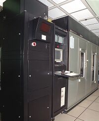
The first full-field step-and-scan 193-nm lithography system was built by SVG Lithography and installed in the Lincoln Laboratory cleanroom facilities (Figure 1).
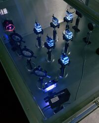
This system's performance was then tested and characterized jointly with IBM and SEMATECH. The first 193-nm acid-catalyzed single-layer photoresists were developed jointly with IBM and patterned at Lincoln Laboratory. A test bed was established and utilized to evaluate the long-term performance of optical lens materials, optical coatings, and pellicle membranes; the information obtained in this manner assisted commercial suppliers employed in 193-nm projection systems, including Corning, Heraeus, and Shin-Etsu, to improve their products (Figure 2).

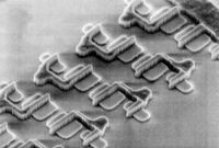
The first lithography-grade 193-nm excimer laser was built by Cymer Laser and integrated in the Lincoln Laboratory facility. The first electrically functional ring oscillators were fabricated at Lincoln Laboratory, thus demonstrating the feasibility of the eventual fabrication of integrated circuits (Figure 3).

Indeed, the 193-nm lithography pioneered at Lincoln Laboratory has been the engine powering the whole semiconductor industry worldwide, enabling the fabrication of every chip in every leading-edge laptop, smartphone, military system, or data center for the last 20 years.
What obstacles (technical, political, geographic) needed to be overcome?
The very concept of 193-nm projection lithography was initially met with skepticism and outright derision. The reasons were both technical and organizational. At the technical level, optics experts did not believe that high-transparency, high-performance lens materials could ever be obtained. Similarly, photoresist experts did not believe that high-transparency, etch-resistant resists could be developed. On the organizational side, Lincoln Laboratory was not known as a powerhouse in lithography or semiconductor processing, unlike groups at IBM or Bell Laboratories. Furthermore, the general consensus in the lithography community was that next-generation lithography would be radically different, i.e., proximity X-ray lithography, not projection UV lithography. Large amounts of money and manpower had been invested in X-ray lithography, and its commercial feasibility seemed to be within reach when the Lincoln Laboratory team proposed exploring 193-nm lithography. Thus, both the conventional wisdom and the momentum did not favor 193-nm lithography in the mid-1980s. Nevertheless, by 1994−1995 the tide had turned. X-ray lithography was being abandoned, and 193-nm was viewed, correctly, as the next lithography technology.
What features set this work apart from similar achievements?
This multifaceted work included breakthroughs in multiple areas, which then combined to a groundbreaking whole. It included the identification of laser-induced nonlinear processes in fused silica, namely color center formation and volumetric compaction, followed by their quantitative systematic characterization to enable optimization of lens materials. It also included the development of a polymeric single-layer resist with the appropriate photosensitivity and etch resistance, the characterization of high-performance projection optics, the demonstration of layer-to-layer alignment, and the end-to-end fabrication of electrically active devices at dimensions that were state of the art at the time. A related unique feature of this project was the close collaboration with all the organizations throughout the supply chain, from lens makers to laser manufacturers, resist chemists, lithography system suppliers, as well as the eventual users of this technology, the semiconductor manufacturers. This collaboration took multiple forms, from having assignees from IBM and SEMATECH integrated in the Lincoln Laboratory team, to a collaborative development program with SVG Lithography, to data sharing with Corning, Heraeus, Shin-Etsu, DuPont, Shipley, and others, and to direct funding by both SEMATECH and the Department of Defense. The project also included semi-annual reviews by a steering group made up of representatives of the semiconductor manufacturers, with the Lincoln Laboratory team actively addressing the feedback provided by them.
Why was the achievement successful and impactful?
Supporting texts and citations to establish the dates, location, and importance of the achievement: Minimum of five (5), but as many as needed to support the milestone, such as patents, contemporary newspaper articles, journal articles, or chapters in scholarly books. 'Scholarly' is defined as peer-reviewed, with references, and published. You must supply the texts or excerpts themselves, not just the references. At least one of the references must be from a scholarly book or journal article. All supporting materials must be in English, or accompanied by an English translation.
References:
[1] D.J. Ehrlich, J.Y. Tsao, and C.O. Bozler, “Submicrometer patterning by projected excimer-laser-beam induced chemistry,” Journal of Vacuum Science and Technology B, vol. 3, no. 1, pp. 1-8, Jan/Feb 1985. Media:IEEE_Milestone_REFERENCE_1.pdf
[2] M. Rothschild and D.J. Ehrlich, “A review of excimer laser projection lithography,” Journal of Vacuum Science and Technology B, vol. 6, no. 1, pp. 1-17, Jan/Feb 1988. Media:IEEE_Milestone_REFERENCE_2.pdf
[3] M. Rothschild, R.B. Goodman, M.A. Hartney, M.W. Horn, R.R. Kunz, J.H.C. Sedlacek, and D.C. Shaver, “Photolithography at 193 nm,” Journal of Vacuum Science and Technology B, vol. 10, no. 6, pp. 2989-2996, Nov/Dec 1992. Media:IEEE_Milestone_REFERENCE_3.pdf
[4] M. Rothschild, A. R. Forte, M.W. Horn, R.R. Kunz, S.C. Palmateer, and J.H.C. Sedlacek, “193-nm lithography (Review Paper),” Proceedings of SPIE, vol. 2703, pp. 398-404, 1996. Media:IEEE_Milestone_REFERENCE_4.pdf
[5] J. A. Burns, C. L. Keast, J. M. Knecht, R. R. Kunz, S. C. Palmateer, S. Cann, A. Soares, and D. C. Shaver, “Performance of a low power fully-depleted deep submicron SOI technology and its extension to 0.15 µm,” Proceedings 1996 IEEE International SOI Conference, Oct. 1996, pp. 102-103, 1996. Media:IEEE_Milestone_REFERENCE_5.pdf
[6] M. Rothschild, J.A. Burns, S.G. Cann, A.R. Forte, C.L. Keast, R.R. Kunz, S.C. Palmateer, J.H.C. Sedlacek, R. Uttaro, A. Grenville, and D. Corliss, “How practical is 193 nm lithography?” Journal of Vacuum Science and Technology B, vol. 14, no. 6, pp. 4157-4161, Nov/Dec 1996. Media:IEEE_Milestone_REFERENCE_6.pdf
[7] M. Rothschild, M.W. Horn, C.L. Keast, R.R. Kunz, V. Liberman, S.C. Palmateer, S.P. Doran, A.R. Forte, R.B. Goodman, J.H.C. Sedlacek, R.S. Uttaro, D. Corliss, and A. Grenville, “Photolithography at 193 nm,” The Lincoln Laboratory Journal, vol. 10, no. 1, pp. 19-34, 1997. Media:IEEE_Milestone_REFERENCE_7.pdf
Supporting materials (supported formats: GIF, JPEG, PNG, PDF, DOC): All supporting materials must be in English, or if not in English, accompanied by an English translation. You must supply the texts or excerpts themselves, not just the references. For documents that are copyright-encumbered, or which you do not have rights to post, email the documents themselves to ieee-history@ieee.org. Please see the Milestone Program Guidelines for more information.
Letters of support:
(1) Support letter from the Director of MIT Lincoln Laboratory. Media:MIT_LL_Support_Letter_IEEE_Milestone_MIT_LL_Development_of_193-nm_Projection_Photolithography.pdf
(2) Support letter from the Chair of the Boston Section of the IEEE. Media:Section_Chair_Support_Letter_IEEE_Milestone_MIT_LL_Development_of_193-nm_Projection_Photolithography.pdf
(3) Support from the IEEE Electron Devices Society: President, Ravi M. Todi, Western Digital Media:IEEE_EDS_Support_Letter_IEEE_Milestone_MIT_LL_Development_of_193-nm_Projection_Photolithography.pdf
(4) Support from the IEEE Electron Devices Society, Optoelectronic Devices Technical Committee: Chair, Prof. Jamie Phillips Media:IEEE_EDS_OD_TC_Support_Letter_IEEE_Milestone_MIT_LL_Development_of_193-nm_Projection_Photolithography.pdf
(5) Support letter from the IEEE Boston Section Affinity Group for Life Members: Chair, Lori Jeromin
Media:Section_Life_Members_Support_Letter_IEEE_Milestone_MIT_LL_Development_of_193-nm_Projection_Photolithography.pdf
Please email a jpeg or PDF a letter in English, or with English translation, from the site owner(s) giving permission to place IEEE milestone plaque on the property, and a letter (or forwarded email) from the appropriate Section Chair supporting the Milestone application to ieee-history@ieee.org with the subject line "Attention: Milestone Administrator." Note that there are multiple texts of the letter depending on whether an IEEE organizational unit other than the section will be paying for the plaque(s). Please recommend reviewers by emailing their names and email addresses to ieee-history@ieee.org. Please include the docket number and brief title of your proposal in the subject line of all emails.
