File:Optical-materials-research Fig2 Ref7 IEEE Milestone MIT LL Development of 193-nm Projection Photolithography.jpg
Original file (1,200 × 1,500 pixels, file size: 793 KB, MIME type: image/jpeg)
Summary
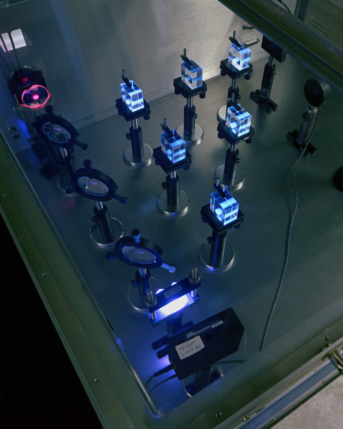
Optical materials research: Samples of fused silica being irradiated at 193 nm in the Lincoln Laboratory test and evaluation facility for optical materials. Research at this facility is being done to quantify the magnitude of various laser-induced effects on optical materials, and their scaling with laser intensity, pulse count, and geometry of irradiation. The visible fluorescence seen above indicates that the fused-silica materials in this experiment are not fully transparent at 193 nm. [Figure 2, Reference 7: THE LINCOLN LABORATORY JOURNAL VOLUME 10, NUMBER 1, 1997, p. 23.]
File history
Click on a date/time to view the file as it appeared at that time.
| Date/Time | Thumbnail | Dimensions | User | Comment | |
|---|---|---|---|---|---|
| current | 21:42, 25 April 2022 | | 1,200 × 1,500 (793 KB) | Joe Campbell (talk | contribs) | Original photo. |
| 18:40, 21 April 2022 |  | 355 × 444 (91 KB) | Joe Campbell (talk | contribs) | Optical materials research: Samples of fused silica being irradiated at 193 nm in the Lincoln Laboratory test and evaluation facility for optical materials. Research at this facility is being done to quantify the magnitude of various laser-induced effects on optical materials, and their scaling with laser intensity, pulse count, and geometry of irradiation. The visible fluorescence seen above indicates that the fused-silica materials in this experiment are not fully transparent at 193 nm. [Fi... |
You cannot overwrite this file.
File usage
The following 2 pages use this file: