Milestones:Development of 193-nm Projection Photolithography
This is a temporary page. The final version of this page can be found on the Engineering and Technology History Wiki
Title
Development of 193-nm Projection Photolithography, 1984-1996
Citation
MIT Lincoln Laboratory pioneered the research, development, and demonstration of 193-nm projection lithography. This technology became the dominant high-resolution patterning technique, enabling the continuous performance scaling of integrated circuits for decades. During 1984–1996, Lincoln Laboratory established an international research center with industrial partners and consortia to guide microelectronic chip manufacturing with 193-nm lithography, which paved the way for its widespread commercial adoption.
Street address(es) and GPS coordinates of the Milestone Plaque Sites
244 Wood Street, Lexington, MA 02421 (Main Lobby coordinates in decimal degrees: 42.459061, -71.266997), 244 Wood Street, Lexington, MA 02421 (Main Lobby coordinates in decimal degrees: 42.459061, -71.266997)
Details of the physical location of the plaque
In a display case in the Main Lobby of MIT Lincoln Laboratory
How the intended plaque site is protected/secured
MIT Lincoln Laboratory is a secure facility. It has gated access that requires identification to enter. The main entrance and lobby area are open to the public (with identification).
Historical significance of the work
This pioneering work from 1984–1996 on 193-nm projection photolithography demonstrated the feasibility and the practicality of all aspects of this technology for high-volume manufacturing of advanced semiconductor integrated circuits. It enabled the semiconductor industry to stay on the path charted by Moore’s law since ~2000 for nearly two decades. Starting in 1984, MIT Lincoln Laboratory demonstrated 193-nm laser-induced patterning in projection mode. Despite initial widespread skepticism throughout the semiconductor industry, from 1988 on, Lincoln Laboratory became the international center of excellence to develop this technology. Lincoln Laboratory addressed all major science and engineering aspects, from materials science to polymer chemistry, optical engineering, and system integration.
Significant milestones leading to the development of 193-nm projection photolithography include:
• 1984: First projection patterning with 193-nm microstepper<br> • 1987: First projection patterning of polymeric photoresists at 193 nm<br> • 1994: First full-field 193-nm step-and-scan system operational<br> • 1996: First functional electronic devices fabricated with 193-nm projection lithography<br> • 1996: First demonstration of phase shifting masks in 193-nm projection lithography
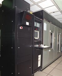
The first full-field step-and-scan 193-nm lithography system was built by SVG Lithography and installed in the Lincoln Laboratory cleanroom facilities (Figure 1).
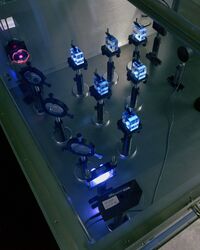
This system's performance was then tested and characterized jointly with IBM and SEMATECH. The first 193-nm acid-catalyzed single-layer photoresists were developed jointly with IBM and patterned at Lincoln Laboratory. A test bed was established and utilized to evaluate the long-term performance of optical lens materials, optical coatings, and pellicle membranes; the information obtained in this manner assisted commercial suppliers employed in 193-nm projection systems, including Corning, Heraeus, and Shin-Etsu, to improve their products (Figure 2).

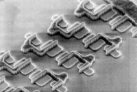
The first lithography-grade 193-nm excimer laser was built by Cymer Laser and integrated in the Lincoln Laboratory facility. The first electrically functional ring oscillators were fabricated at Lincoln Laboratory, thus demonstrating the feasibility of the eventual fabrication of integrated circuits (Figure 3).

Indeed, the 193-nm lithography pioneered at Lincoln Laboratory has been the engine powering the whole semiconductor industry worldwide, enabling the fabrication of every chip in every leading-edge laptop, smartphone, military system, or data center for the last 20 years.
Features that set this work apart from similar achievements
This multifaceted work included breakthroughs in multiple areas, which then combined to a groundbreaking whole. It included the identification of laser-induced nonlinear processes in fused silica, namely color center formation and volumetric compaction, followed by their quantitative systematic characterization to enable optimization of lens materials. It also included the development of a polymeric single-layer resist with the appropriate photosensitivity and etch resistance, the characterization of high-performance projection optics, the demonstration of layer-to-layer alignment, and the end-to-end fabrication of electrically active devices at dimensions that were state of the art at the time. A related unique feature of this project was the close collaboration with all the organizations throughout the supply chain, from lens makers to laser manufacturers, resist chemists, lithography system suppliers, as well as the eventual users of this technology, the semiconductor manufacturers. This collaboration took multiple forms, from having assignees from IBM and SEMATECH integrated in the Lincoln Laboratory team, to a collaborative development program with SVG Lithography, to data sharing with Corning, Heraeus, Shin-Etsu, DuPont, Shipley, and others, and to direct funding by both SEMATECH and the Department of Defense. The project also included semi-annual reviews by a steering group made up of representatives of the semiconductor manufacturers, with the Lincoln Laboratory team actively addressing the feedback provided by them.
Significant references
References:<p> [1] D.J. Ehrlich, J.Y. Tsao, and C.O. Bozler, “Submicrometer patterning by projected excimer-laser-beam induced chemistry,” <i>Journal of Vacuum Science and Technology B,</i> vol. 3, no. 1, pp. 1-8, Jan/Feb 1985. Media:IEEE_Milestone_REFERENCE_1.pdf <br> [2] M. Rothschild and D.J. Ehrlich, “A review of excimer laser projection lithography,” <i>Journal of Vacuum Science and Technology B,</i> vol. 6, no. 1, pp. 1-17, Jan/Feb 1988. Media:IEEE_Milestone_REFERENCE_2.pdf <br> [3] M. Rothschild, R.B. Goodman, M.A. Hartney, M.W. Horn, R.R. Kunz, J.H.C. Sedlacek, and D.C. Shaver, “Photolithography at 193 nm,” <i>Journal of Vacuum Science and Technology B,</i> vol. 10, no. 6, pp. 2989-2996, Nov/Dec 1992. Media:IEEE_Milestone_REFERENCE_3.pdf <br> [4] M. Rothschild, A. R. Forte, M.W. Horn, R.R. Kunz, S.C. Palmateer, and J.H.C. Sedlacek, “193-nm lithography (Review Paper),” <i>Proceedings of SPIE,</i> vol. 2703, pp. 398-404, 1996. Media:IEEE_Milestone_REFERENCE_4.pdf <br> [5] J. A. Burns, C. L. Keast, J. M. Knecht, R. R. Kunz, S. C. Palmateer, S. Cann, A. Soares, and D. C. Shaver, “Performance of a low power fully-depleted deep submicron SOI technology and its extension to 0.15 µm,” <i>Proceedings 1996 IEEE International SOI Conference,</i> Oct. 1996, pp. 102-103, 1996. Media:IEEE_Milestone_REFERENCE_5.pdf <br> [6] M. Rothschild, J.A. Burns, S.G. Cann, A.R. Forte, C.L. Keast, R.R. Kunz, S.C. Palmateer, J.H.C. Sedlacek, R. Uttaro, A. Grenville, and D. Corliss, “How practical is 193 nm lithography?” <i>Journal of Vacuum Science and Technology B,</i> vol. 14, no. 6, pp. 4157-4161, Nov/Dec 1996. Media:IEEE_Milestone_REFERENCE_6.pdf <br> [7] M. Rothschild, M.W. Horn, C.L. Keast, R.R. Kunz, V. Liberman, S.C. Palmateer, S.P. Doran, A.R. Forte, R.B. Goodman, J.H.C. Sedlacek, R.S. Uttaro, D. Corliss, and A. Grenville, “Photolithography at 193 nm,” <i>The Lincoln Laboratory Journal,</i> vol. 10, no. 1, pp. 19-34, 1997. Media:IEEE_Milestone_REFERENCE_7.pdf <p>
Supporting materials
<p>Letters of support:<p> (1) Support letter from the Director of MIT Lincoln Laboratory. Media:MIT_LL_Support_Letter_IEEE_Milestone_MIT_LL_Development_of_193-nm_Projection_Photolithography.pdf <br> (2) Support letter from the Chair of the Boston Section of the IEEE. Media:Section_Chair_Support_Letter_IEEE_Milestone_MIT_LL_Development_of_193-nm_Projection_Photolithography.pdf <br> (3) Support from the IEEE Electron Devices Society: President, Ravi M. Todi, Western Digital Media:IEEE_EDS_Support_Letter_IEEE_Milestone_MIT_LL_Development_of_193-nm_Projection_Photolithography.pdf <br> (4) Support from the IEEE Electron Devices Society, Optoelectronic Devices Technical Committee: Chair, Prof. Jamie Phillips Media:IEEE_EDS_OD_TC_Support_Letter_IEEE_Milestone_MIT_LL_Development_of_193-nm_Projection_Photolithography.pdf <br> (5) Support letter from the IEEE Boston Section Affinity Group for Life Members: Chair, Lori Jeromin Media:Section_Life_Members_Support_Letter_IEEE_Milestone_MIT_LL_Development_of_193-nm_Projection_Photolithography.pdf <p>
