File:First-transistors ring-oscillator IEEE Milestone MIT LL Development of 193-nm Projection Photolithography.png

Original file (3,000 × 2,018 pixels, file size: 2.64 MB, MIME type: image/jpeg)
Summary
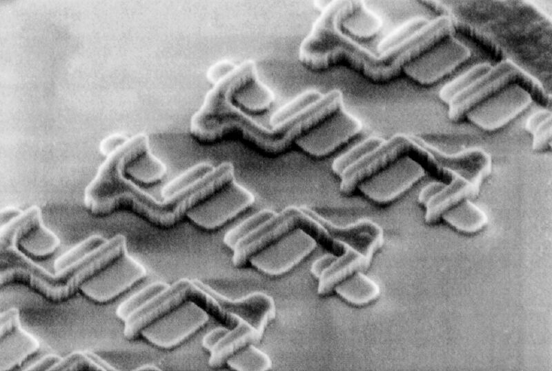
First transistors, ring oscillator: Scanning electron micrographs of 200-nm polysilicon transistor gates patterned over 50-nm-thick silicon islands, all on a substrate of silicon dioxide on a silicon wafer. The gates were patterned by using the silylation top-surface-imaged resist process. When these devices were fully fabricated, the maximum switching speed measured from a 49-stage ring oscillator was 29 psec when the devices were run at 3 V and 57 psec when they were run at 1 V, indicating successful processing. [Figure 6, Reference 7: THE LINCOLN LABORATORY JOURNAL VOLUME 10, NUMBER 1, 1997, p. 28.]
File history
Click on a date/time to view the file as it appeared at that time.
| Date/Time | Thumbnail | Dimensions | User | Comment | |
|---|---|---|---|---|---|
| current | 21:47, 25 April 2022 | | 3,000 × 2,018 (2.64 MB) | Joe Campbell (talk | contribs) | Original scanning electron micrograph. |
| 18:32, 21 April 2022 | 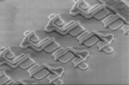 | 550 × 363 (142 KB) | Joe Campbell (talk | contribs) | First transistors, ring oscillator: Scanning electron micrographs of 200-nm polysilicon transistor gates patterned over 50-nm-thick silicon islands, all on a substrate of silicon dioxide on a silicon wafer. The gates were patterned by using the silylation top-surface-imaged resist process. When these devices were fully fabricated, the maximum switching speed measured from a 49-stage ring oscillator was 29 psec when the devices were run at 3 V and 57 psec when they were run at 1 V, indicating... |
You cannot overwrite this file.
File usage
The following 2 pages use this file: