Milestone-Proposal:Vertical-Cavity Surface-Emitting Laser, 1977
To see comments, or add a comment to this discussion, click here.
Docket #:2022-11
This proposal has been submitted for review.
To the proposer’s knowledge, is this achievement subject to litigation? No
Is the achievement you are proposing more than 25 years old? Yes
Is the achievement you are proposing within IEEE’s designated fields as defined by IEEE Bylaw I-104.11, namely: Engineering, Computer Sciences and Information Technology, Physical Sciences, Biological and Medical Sciences, Mathematics, Technical Communications, Education, Management, and Law and Policy. Yes
Did the achievement provide a meaningful benefit for humanity? Yes
Was it of at least regional importance? Yes
Has an IEEE Organizational Unit agreed to pay for the milestone plaque(s)? Yes
Has the IEEE Section(s) in which the plaque(s) will be located agreed to arrange the dedication ceremony? Yes
Has the IEEE Section in which the milestone is located agreed to take responsibility for the plaque after it is dedicated? Yes
Has the owner of the site agreed to have it designated as an IEEE Milestone? Yes
Year or range of years in which the achievement occurred:
1977-1992
Title of the proposed milestone:
Vertical-Cavity Surface-Emitting Laser, 1977-1992
Plaque citation summarizing the achievement and its significance; if personal name(s) are included, such name(s) must follow the achievement itself in the citation wording: Text absolutely limited by plaque dimensions to 70 words; 60 is preferable for aesthetic reasons.
The Vertical-Cavity Surface-Emitting Laser (VCSEL), conceived by Kenichi Iga at Tokyo Institute of Technology in 1977, is notable for its single-mode operation, easy monolithic manufacturability, and frequency tunability. Iga’s team demonstrated the first current-driven VCSEL in 1979, room temperature continuous operation in 1988, and mechanical continuous-frequency tuning in 1992. VCSELs became widely used in applications such as data communications, laser printing, facial recognition, and LiDAR.
200-250 word abstract describing the significance of the technical achievement being proposed, the person(s) involved, historical context, humanitarian and social impact, as well as any possible controversies the advocate might need to review.
On March 22, 1977, Kenichi Iga of Tokyo Institute of Technology conceived a surface-emitting laser with light output vertically from the wafer surface, unlike the conventional edge-emitting laser. His research aimed to realize a current-injection semiconductor laser that achieved (i) stable single-frequency oscillation, (ii) monolithic manufacturability, and (iii) continuous frequency tunability. This device was later named the vertical-cavity surface-emitting laser (VCSEL). Iga's team demonstrated the feasibility of VCSELs by achieving laser oscillation with this new structure in 1979. Through innovative and persistent research, Iga's team made significant advancements in VCSEL performance and production. They achieved the first room temperature continuous operation, very low threshold and driving currents, circular light beams, and confirmed the three key goals: stable single-frequency oscillation, monolithic fabrication, and continuous frequency tuning. The initially demonstrated array formation allowed for wafer-scale testing, enhancing device fabrication efficiency. Iga also promoted VCSELs globally through lectures, broadening their application from communications to consumer electronics. The VCSEL has since become a key component in advancing the information society of the 21st century. From conception to technological development and commercialization, Iga's contributions were substantial and irreplaceable. For this work, Iga was awarded the 2021 IEEE Edison Medal and other honors.
IEEE technical societies and technical councils within whose fields of interest the Milestone proposal resides.
IEEE Photonics Society
In what IEEE section(s) does it reside?
IEEE Tokyo Section
IEEE Organizational Unit(s) which have agreed to sponsor the Milestone:
IEEE Organizational Unit(s) paying for milestone plaque(s):
Unit: IEEE Tokyo Section
Senior Officer Name: Dr. Kiyoharu Aizawa
IEEE Organizational Unit(s) arranging the dedication ceremony:
Unit: IEEE Tokyo Section
Senior Officer Name: Dr. Kiyoharu Aizawa
IEEE section(s) monitoring the plaque(s):
IEEE Section: IEEE Tokyo Section
IEEE Section Chair name: Dr. Kiyoharu Aizawa
Milestone proposer(s):
Proposer name: Kohroh Kobayashi
Proposer email: Proposer's email masked to public
Proposer name: Fumio Koyama
Proposer email: Proposer's email masked to public
Please note: your email address and contact information will be masked on the website for privacy reasons. Only IEEE History Center Staff will be able to view the email address.
Street address(es) and GPS coordinates in decimal form of the intended milestone plaque site(s):
Milestone plaque site: 35.5154784, 139.4824420
Tokyo Institute of Technology, Suzukake-dai Campus 4259 Nagatsuta, Midori-ku, Yokohama, 226-8501, Japan
Milestone plaque replica site: 35.606876,139,684802
Tokyo Institute of Technology Museum
Describe briefly the intended site(s) of the milestone plaque(s). The intended site(s) must have a direct connection with the achievement (e.g. where developed, invented, tested, demonstrated, installed, or operated, etc.). A museum where a device or example of the technology is displayed, or the university where the inventor studied, are not, in themselves, sufficient connection for a milestone plaque.
Please give the details of the mounting, i.e. on the outside of the building, in the ground floor entrance hall, on a plinth on the grounds, etc. If visitors to the plaque site will need to go through security, or make an appointment, please give the contact information visitors will need. 1) Milestone plaque:
The milestone plaque will reside in the Suzukake-dai campus of Tokyo Institute of Technology, 4259 Nagatsuta, Midori-ku, Yokohama, 226-8501 Japan.
2) Milestone replica plaque:
The replica plaque will be displayed in the Institute Museum at O-okayama Campus,Tokyo Institute of Technology.
Are the original buildings extant?
Yes, Professor Kenichi Iga’s laboratories existed in the main building of the FIRST (Future Interdisciplinary Research of Science and Technology) Laboratory (Building R2) at Suzukake-dai Campus of Tokyo Institute of Technology in 1975-Present.
Details of the plaque mounting:
1) Milestone plaque: The milestone plaque will reside in the Suzukake-dai campus of Tokyo Institute of Technology. The plaque will be installed on the ground along the way from the campus entrance to the FIRST building where Professor Kenichi Iga’s laboratories existed. The plaque site is in proximity to the FIRST building and is supposed to be located next to the Milestone plaque of Koga’s temperature-insensitive quartz oscillation plate. Both milestone plaques will be fixed on each heavy stone monument.
2) Milestone replica plaque: The replica plaque will be displayed in the special showcase at the Exhibition Room of the Institute Museum at O-okayama Campus, Tokyo Institute of Technology, 2-12-1, O-okayama, Meguro-ku, Tokyo 152-8550, Japan
How is the site protected/secured, and in what ways is it accessible to the public?
Visitors are subject to entrance security protocols for both Milestone plaque site and Milestone plaque replica site.
1) Milestone plaque site: Ground floor in front of FIRST Laboratory
The plaque is open to the public when the Suzukake-dai campus is open, i. e., open weekdays 8:30-17:15. The plaque is protected by a heavy stone monument.
2) Milestone replica site: Institute Museum
The museum is open to the public on weekdays from 10:30 to 16:30. Closed nights and holidays.
Who is the present owner of the site(s)?
Tokyo Institute of Technology National University Corporation
What is the historical significance of the work (its technological, scientific, or social importance)? If personal names are included in citation, include detailed support at the end of this section preceded by "Justification for Inclusion of Name(s)". (see section 6 of Milestone Guidelines)
(1) Scientific: The conception and pioneering study of vertical-cavity surface-emitting laser (VCSEL)
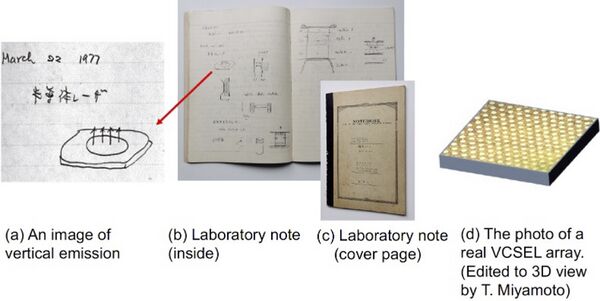
In 1977, Kenichi Iga of Tokyo Institute of Technology conceived a unique semiconductor laser whose simple drawing is shown in Fig. 1 [A1]. Contrary to the conventional Fabry-Perot edge-emitting semiconductor lasers, his idea comprises a laser cavity which is short and vertical to a wafer surface. It was later named VCSEL (Vertical-Cavity Surface-Emitting Laser).
Iga was dissatisfied with the edge-emitting semiconductor lasers from the viewpoints of their fabrication and device characterization. The laser cavity of conventional semiconductor lasers used to be fabricated by manually cleaving wafers in a specific crystal plane. Cavity formation by the cleaving was time consuming and not suited volume production. As far as the laser performance was concerned, spectral characteristics such as single frequency oscillation and its tunability were serious issues to be realized. Toward ideal semiconductor lasers, Kenichi Iga considered three requirements as follows [A2], [A3].
(i) The oscillation frequency should be single.
(ii) The laser should be manufactured by a monolithic process.
(iii) The oscillation frequency should be tunable.
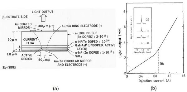
Before the VCSEL was conducted, Iga and Y. Takahashi (graduate student) had analyzed the single-frequency oscillation of a semiconductor laser at high-speed pulse modulation in 1976[A4]. After struggling contemplation to solve these issues, Iga was hit by a conception of the laser cavity vertical to the wafer surface as shown in Fig. 1 [A1]. He immediately suggested some current injection schemes. Introduction of a vertical cavity, monolithic cavity fabrication became possible. Furthermore, a short cavity as short as a wavelength order was easy to realize. Such a short cavity led to single frequency oscillation and to emission frequency tunability. Based on the idea of VCSEL, Iga and his team promoted analytical and experimental research on this new device. The concept and the first experimental results on spontaneous vertical light emission from GaInAsP/InP diodes were presented by Iga at the Spring Meeting of Applied Physics Societies, Japan, March 1978 [A5]. Almost the same content was orally presented in November 1978 at the Fall Meeting of the Applied Physics Societies, Japan[A6]. In 1979, H. Soda (Iga’s graduate student) successfully demonstrated lasing operation of a GaInAsP/InP VCSEL under pulsed injection current condition at 77 K [A7]. The cross-sectional structure and light output vs. current characteristics are shown in Fig. 2. This is the first demonstration of the current-injected VCSEL lasing oscillation, which clearly showed the possibility of a VCSEL as a practical vertical-cavity laser. Iga and his team concentrated on paving the way for this new and attractive semiconductor laser.
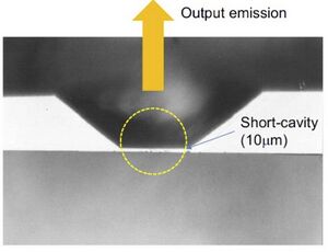
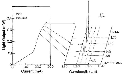
Following the world’s first lasing of a VCSEL, Iga, Y. Motegi and H. Soda (graduate students) made a breakthrough by fabricating a short cavity of about 10-micron long [A8]. They developed a fine chemical etching technology to realize such a short cavity length. The image of the cross section is shown in Fig. 3. A flat-enough surface was obtained for laser resonator formation. The emission spectra under pulsed current excitation at 77 K are shown in Fig. 4. A single-longitudinal-mode oscillation was maintained up to at least 1.7 times the threshold. The longitudinal-mode spacing was large(175 Å), reflecting the short cavity length. As mentioned before, the theoretical simulation had pointed out that a short-cavity is effective in achieving single-frequency oscillation [A4]. Their theory was confirmed by this experiment with a short-cavity VCSEL [A8].
In 1986, Iga’s graduate student, S. Kinoshita succeeded in reducing the threshold current of VCSELs to less than 10 mA for the first time in the world [A9], [A10]. The threshold current was 4.5 mA at 77 K under CW current and 6 mA at room temperature under pulsed injection, with a buried hetero-structure AlGaAs/GaAs VCSEL. This low-threshold current achievement was paid attention from the community of semiconductor lasers.
Since then, Iga and his team have been continuously conducting elaborate research and development on VCSELs and achieved many results, which have contributed to the growth of VCSEL devices and related applications. Theoretical and experimental studies for VCSELs done by Iga’s team were summarized as a paper in IEEE Journal of Quantum Electronics in 1988 [A11]. Based on the research results, dynamic single frequency operation, extremely low threshold current of <1 mA, and a possibility of room temperature CW operation of VCSELs were predicted in the paper. Fundamental results on a 5x5 two-dimensional array were also described. This paper is marked as the highest citation in the VCSEL area.
(2) Technological: Device realization including semiconductor crystal growth, nanofabrication, and theoretical and experimental study on the physics of short-cavity lasers for single mode operation.
(i) Stable single-frequency operation of VCSELs
Iga had suggested through theoretical analysis that a single-frequency oscillation is possible by making cavity length being less than several tens of micron even at high-speed pulse modulation [A4]. In 1982, Iga,s graduate-student, Motegi and Soda successfully demonstrated a single-frequency operation for the first time in the world. They used a GaInAsP/InP double heterostructure with a cavity length of about 10 microns by etching a substrate off [A8].
(ii) Continuous-wave operation at room temperature
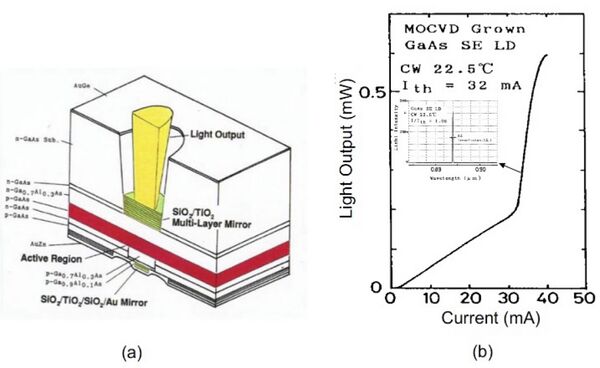
Continuous-wave (CW) operation at room temperature is one of the criteria for the device to be acknowledged as applicable to equipment and systems. In the case of VCSELs, more than ten years have passed from the conception in 1977[A1] to obtain the CW oscillation at room temperature. It was achieved by Fumio Koyama of Iga’s team in 1988 [A12]. They used an AlGaAs/GaAs VCSEL structure with a micro-cavity made of dielectric multilayer mirrors at the wavelength of 0.8 microns as shown in Fig. 5(a). The threshold current was about 30 mA at room temperature as shown in Fig.5(b).
The first room-temperature CW operation of long-wavelength VCSEL was also achieved by T. Baba of Iga’s team in 1993 with InGaAsP/InP system and a thermally conductive MgO/Si multilayered mirror [A13]. The emission wavelength was 1.2 microns.
(iii) Low-threshold-current laser operation
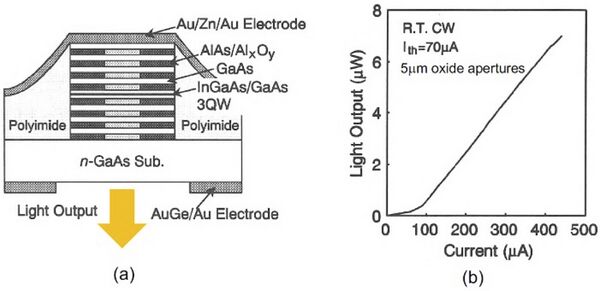
Many researchers in the world have striven to further reduce the threshold current. In 1995, Iga’s team again achieved the record low threshold current of 70 μA in native oxide-confined index-guided VCSELs (Fig. 6) [A14]. Their effort and results have significantly accelerated the development and progress of VCSELs.
(iv) Introduction of MQW active region into VCSEL
As a higher gain medium for VCSELs, an AlGaAs/GaAs MQW structure was first introduced into VCSELs by Kenichi Iga, and H. Uenohara (graduate student) in 1987 [A15], [A16]. After this trial, a single-quantum well or an MQW has become a standard active medium in VCSELs.
(v) Semiconductor multilayered Bragg reflector
The semiconductor multilayered Bragg reflector was also first introduced by Iga as one of the mirrors for a laser vertical cavity. The first VCSEL with this semiconductor mirror was successfully demonstrated by Iga’s team with an AlGaAs/AlAs multilayered Bragg reflector in 1988 [A17]. This enabled the fabrication of lasers with full monolithic semiconductor processing, which drastically improved the productivity of laser fabrication. This is really one of the advantages that Iga desired to realize with the VCSEL configuration.
(vi) Continuous-frequency tuning
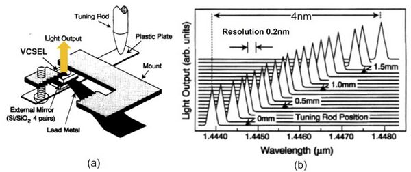
Owing to the short cavity length, a VCSEL emits single-frequency light defined by the cavity length. Continuous-frequency tuning was demonstrated by N. Yokouchi, graduate student of Iga’s team with an InGaAsP/InP VCSEL, one of the mirrors of which was replaced by a mechanically movable external mirror in 1992 as depicted in Fig. 7 [A18], [A19]. The wavelength was continuously changed over 40 Å at 77 K. This study was followed by a monolithic version, Micro- Electro-Mechanical System (MEMS) of frequency-tunable VCSEL in later time [B28].
(vii)Two-dimensional array
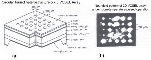
The surface emitting laser enables a two-dimensional array formation. Iga’s team tried to realize two-dimensional VCSEL arrays and demonstrated a 2x2 array in 1985 [A20] and a 5x5 array in 1988 [A11]. The structure and emission pattern of a 5x5 array are shown in Fig. 8 [A11]. All the VCSEL devices are simultaneously driven by one electrical contact in this experiment. This feasibility trial for the array formation encouraged people toward high productivity by making possible chip characterization on a wafer scale. The two-dimensional VCSEL array configuration was industrialized later in high-density and high-speed laser printers in 2001.
(3) Social: Social importance of the proposal and development of VCSELs
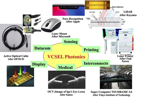
Besides the room-temperature continuous-wave (CW) operation of VCSELs[A12], which is indispensable to the industrialization of devices, many disruptive features of VCSELs such as high productivity, high efficiency, low power consumption, a circular beam, a single frequency, and a two-dimensional array, all of which were realized by Iga’s team, are becoming well-recognized worldwide, and their application areas have been expanding since the mid-1990s. The VCSEL applications are shown in Fig. 9 [A2], [A3], [A22], [A23]. The application areas started with data communications, followed by sensors, printers, and computer mouse pointers until the mid-2010s. Since then, although the market size of data communication and sensing has steadily grown and is still expected to grow and occupy the main body of the VCSEL’s markets and related ones, VCSELs are exploring applications in new areas such as face recognition and LiDARs (Light Detection And Ranging) for automatic driving, infrared illumination, pumping, and industrial heating.
These applications will provide huge potential for VCSEL markets. VCSELs are the most suitable light sources for these applications because of their advantageous features such as low cost owing to high productivity, high reliability, low power consumption, small size, and ease of two-dimensional array integration. As described here, VCSELs are becoming indispensable key components, which support the information society for today and the future from data-com to smart sensing. It is not easy to imagine societies without VCSELs.
Justification of Name in the Citation
Kenichi Iga first conceived the vertical-cavity semiconductor laser in 1977, a concept that has been foundational to modern devices. This innovation introduced single-mode operation through a short cavity, facilitated 2D array manufacturing due to the vertical cavity, and enabled wide continuous frequency tuning via a large free spectral range (FSR). Iga’s team demonstrated the feasibility of this technology by achieving the first current-driven device in 1979, and later achieving room-temperature continuous-wave operation in 1988 and mechanical frequency tuning in 1992. In addition to his laboratory achievements, Iga made significant efforts to promote the VCSEL by delivering lectures and talks at universities and companies across the US and Europe. As a pioneer of the VCSEL, he proposed potential applications for this technology in 1988. His distinguished and diverse contributions were recognized with the 2021 IEEE Thomas Edison Medal, among other honors listed below.
Detailed Description
1) Recognition
For the achievement related to this citation, Kenichi Iga received the following honors.
[From IEEE]
2021 IEEE Thomas Edison Medal, 2003 IEEE Daniel E. Noble Award, 2000 IEEE, Millennium Medal, 1998 IEEE/OSA John Tyndall Award, 1992 IEEE/LEOS William Streifer Award for Scientific Achievement,
[From Other Organizations]
2024 OPTICA Frederic Ives Medal/Jarus Quinn Prize, 2013 Franklin Institute’s Bower Award and Prize in Science, 2018 Japanese Emperor “The Order of the Sacred Treasure, Gold and Sliver Star”, 2022 Japanese Government “Person of Cultural Merits”
2) Citations
(a) Kenichi Iga’s citations
From Google Scholar: 17,527, h-Index: 62, i10: 286
(b) Most cited papers from Google Scholar on VCSELs are: [A17] H. Soda, K. Iga*), C. Kitahara and Y. Suematsu, “GaInAsP/InP surface emitting injection lasers,” Jpn. J. Appl. Phys., vol. 18, pp. 2329-2330 (1979) Cited:1010 [A11] K. Iga, F. Koyama, and S. Kinoshita, “Surface Emitting Semiconductor Lasers,” IEEE J. Quantum Electronics, Vol. 24, No. 9, pp. 1845-1855, Sept. 1988. Cited 991 Note) There is no paper found above 900 of citations.
3) In a Book edited by T. P. Lee “Current Trends in Vertical Cavity Surface Emitting Semiconductor Lasers”, World Scientific (1995), many authors cite Iga’s papers as Reference [1] which means that Iga is featured as an initiator of VCSELs. cf, A. Scherer, R. A. Morgan, M. Osinski, C. C. Wu, et al.
4) Note: Background of Iga’s Conception
Kenichi Iga began his research in 1973, after being promoted to Associate Professor (Tenured), with a focus on developing a single-frequency semiconductor laser. His initial idea was to explore the potential of a short-cavity laser to widen the Free Spectral Range (FSR). Drawing on his experience in atomic frequency standard research during his postdoctoral period, he was particularly interested in the frequency stability of lasers. He aimed to achieve frequency tuning similar to that of a Voltage Controlled Crystal Oscillator (VCXO). At the time, Iga was manually cleaving wafers to produce edge-emitting semiconductor lasers and found this process to be unsatisfactory. These experiences and long periods of contemplation led Iga in 1977 to conceive the idea of rotating the laser cavity from horizontal to vertical, which he subsequently named the "surface emitting laser." This marked the beginning of his efforts toward its realization. Within the VCSEL community, Iga is recognized as "The Father of VCSEL" or even "The Grandfather," as noted in Connie Chang-Hasnain's speech at the IEEE Holonyak Medal ceremony in May 2024.
What obstacles (technical, political, geographic) needed to be overcome?
At the beginning of 1970s, semiconductor lasers were extensively studied worldwide as a light source for optical fiber communications. With such efforts, performances of semiconductor lasers were significantly improved, including reliability. Kenichi Iga thought these devices were quite attractive but had some serious disadvantages in their productivity, especially in the stage of future large-volume production. The lasers at that time frame were called edge-emitting laser diodes (EE-LDs). A pair of crystal facets formed the laser cavity in a direction parallel to that of the semiconductor substrate surface. The laser cavity of the semiconductor laser was fabricated by cleaving almost manually a thin semiconductor substrate, on which semiconductor laser structures were formed. This manual process was supposed to be a crucial obstacle to mass production of semiconductor lasers.
Kenichi Iga pointed out another drawback, which would emerge from the essential structure in EE-LDs. No practical wafer-scale inspection was possible in EE-LDs for the device characterization and/or the initial chip selection. Such inspection was only possible after the semiconductor wafer was cleaved and separated into laser bars/chips, because the light from the laser came out through the cleaved mirror facet in a direction parallel to that of the semiconductor substrate. This feature of inspection inevitably degrades the semiconductor laser productivity.
Kenichi Iga solved these problems by inventing a new laser structure in which the laser cavity was formed in a direction perpendicular to the semiconductor substrate surface [A1]. The VCSELs were considered, in principle, to be completely fabricated by efficient semiconductor processes, not only by time-consuming but also costly manual processes. An obstacle to preventing lasing oscillation in VCSELs came from the fact that the active region was limited to be quite thin because of the limitation in the crystal growth in the thickness direction and the limited carrier diffusion length. Kenichi Iga successfully achieved lasing in current-injecting VCSELs for the first time in the world by combining a thin active region with a highly reflective mirror [A4]. Since this breakthrough, he has devoted continuous effort to improve the laser performance of VCSELs. By combining a highly efficient quantum well gain medium with highly reflective semiconductor DBR mirrors, Iga’s team realized high performance and practical VCSELs. The VCSEL devices, fabricated by a fully mass-producible semiconductor monolithic process, were aligned in a two-dimensional array on a wafer and all devices were characterized and inspected one by one in the wafer-scale situation if necessary. Crucial issues of semiconductor laser productivity caused by the fabrication and characterization/inspection process were overcome by the introduction of VCSELs. Iga has overcome the obstacle and paved the road for a new laser source world of VCSELs with ample applications, which have been significantly contributing to the prosperity and welfare of the world.
What features set this work apart from similar achievements?
(i) Early similar works
In 1964, coherent light emission from an InSb bulk surface was reported by Melngailis et al. of Lincoln Laboratory, Massachusetts Institute of Technology[B4], followed by an additional report by the same author in 1965[B5]. Iga began to know that paper far later after the VCSELs became popular. The current injection was longitudinal to the coherent light emission, which was parallel to it. This laser operated at a very low temperature of 10 K with current confinement by an intense magnetic field. Even with such current confinement, the drive current was quite high, i.e., 20 A (=60 kA/cm2) under pulsed conditions. Because a crystal-cleaving technique was not developed at this time, the laser cavity was formed by polishing both surfaces of InSb bulky semiconductor wafers. Any short cavity was not supposed. The longitudinal cavity length was 220 microns. No further significant performance improvement has been realized compared with those of the edge-emitting lasers. Iga met Melngailis later and discussed the above issues. It was said that Melngailis did not deny the Iga’s originality of the VCSEL.
Several other reports have appeared on thin-film semiconductor lasers and related experiments since the 1960s. Most of them are optically pumped or electron-beam-pumped and no practical relations are found with the present VCSELs. These include a thin-film CdSe laser by Stillman et al. of University of Illinois, Urbana, in 1966[B6]; a radiating mirror by Basov et al. of Levedev Physics Institute, Academy of Science, USSR, in 1966[B7]; electron-beam-pumped CdS laser by Packard et al. of 3M Company in 1969[B8]; thin dielectric-coated CdS laser by Smiley et al. of Naval Electronics Laboratory Center, San Diego, in 1971[B9]; optical bistability in thin GaAs film by Gibbs et al. of Bell Laboratories in 1979 [B10]; optically pumped ribbon whisker by Duguay et al. of Bell Laboratories, in 1980[B11]; and optically pumped GaAs thin-film laser under low temperature (<115 K) by Passner et al. of Bell Laboratories in 1980[B12].
As described, prior to the proposal and conception by Kenichi Iga in 1977, there existed several fundamental research on semiconductor lasers emitting light vertically from the surface. Most of these studies, however, read optically pumped or electron-beam-pumped thin-film lasers, which turned out not to extend to the present VCSELs, which Kenichi Iga strove for more than 25 years to establish a new semiconductor laser direction with current injection scheme maintained. The VCSELs developed and commercialized at present are on the line where Iga and his team had paved the way.
(ii) Patent by Tokyo Institute of Technology and Xerox-PARC
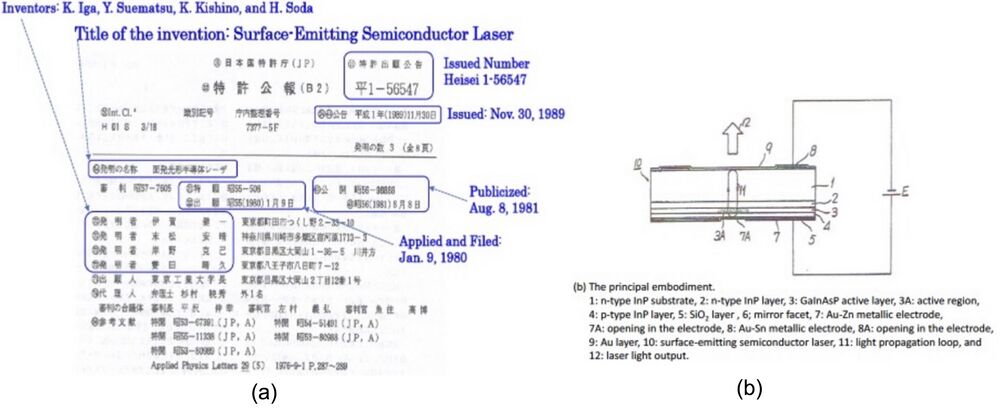
In the initial stage of VCSEL development, two inventions were applied. One was invented by Kenichi Iga et. al, all from Tokyo Institute of Technology, Japan, applied on January 9th, 1980. We call this Titech Patent(Fig, 10)[A21]. Independently from the Titech Patent, R. D. Burnham, D. R. Scifres, and W. Streifer, all from Xerox Corporation, United States of America, applied for a patent on September 13th, 1979. This is called Xerox Patent in this proposal. The title was "Transverse Light Emitting Electroluminescent Devices"[B13].
The said Tokyo Tech Patent and Xerox Patent were granted as independent inventions. Thus, both parties were recognized as independent patent inventors. However, the Xerox patent had not been recognized by most VCSEL research communities until Burnham and Scifres received the 2002 Rank prize as co-recipients together with Iga. On the other hand, Iga received the Streifer Award in 1992 for the VCSEL initiator. This award was established by Xerox in memory of the late William Streifer, who was one of the inventors of the Xerox Patent. The Xerox group performed outstanding work on high-power lasers and edge-emitting DFB lasers, not VCSELs, as far as the nominator knows.
(2) Later similar work
(i) J. Jewell's microlaser
A microlaser was reported by Jewell and his group of AT&T Bell Laboratories[B14]. The active region was a GaInAs 100-Å-thick single-quantum well. The laser cavity was formed by a pair of semiconductor DBR mirrors consisting of AlAs/GaAs multilayers. The threshold currents of 1.3 mA under pulsed condition were reported with a 5-micron square microlaser. The threshold current was reduced to 1.1 mA and 1.5 mA under pulsed and CW current conditions, respectively [B15]. The microlaser was considered as the component of optical computers, which was the mission of Huang’s department at AT&T Bell Labs at that time. Jewell visited Iga’s lab at Tokyo Institute twice: One is just before Koyama and Iga obtained CW operation at room temperature in 1988 and the other is when Iga served as President of Tokyo Institute in 2012. He well recognizes the originality of Iga’s team as the initiator of VCSELs. The nominator appreciates the work of Jewell’s group including A. Scherer, A. C. Gossard, and Y. H. Lee as one of the important players for the promotion of VCSEL toward industrialization.
(ii)Threshold current reduction and device performance progress
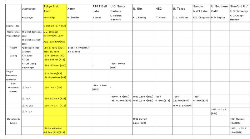
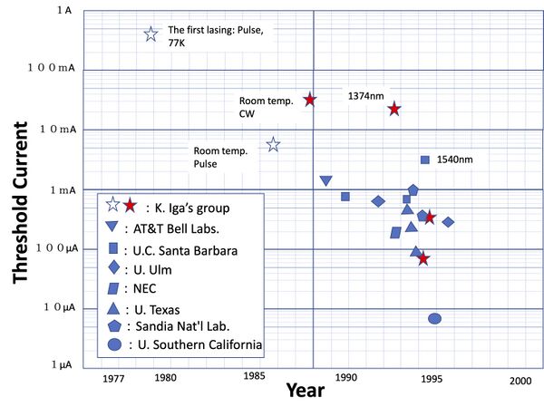
With the hopeful results on VCSEL achieved in the initial feasibility study by Iga and his team many organizations worldwide attracted interest in VCSELs and started research in the 1990s. To show the progress of VCSELs, we track the threshold current reduction by Iga and his team of Tokyo Inst. Tech. and many others from other organizations. Major players and their results on the threshold current are listed in Table I and depicted in Fig. 11. The data were limited to the threshold current under CW conditions at room temperature, except those with a specific remark in the figure. The results achieved by Iga and his team are shown as star marks in Fig. 11. The open stars show threshold current under pulsed current and closed ones show those under CW current.
From the second half of the 1980s to the first half of the 1990s, the threshold current of VCSELs further reduced from a few milliamperes to sub-milliamperes. Jewell et al., of AT&T Bell Laboratories, achieved a low-threshold current of 1.3 mA (pulsed) with three GaInAs quantum wells in 1989[B14]. Soon after that, he announced a CW threshold current as low as 1.5 mA with GaInAs single-quantum well and 5-micron square micro-post structure, as described in (i) in this section[B15]. Geels and Coldren of U. C. Santa Barbara reported the threshold current of 0.7 mA in a VCSEL with a strained InGaAs single-quantum-well active region [B17], that is is the first report for threshold current less than 1 mA. A few years later, they claimed the threshold current of 290 µA[B25]. In 1993, Numai et al., of NEC, achieved a threshold current as low as 190 µA under pulsed condition at room temperature with an InGaAs/GaAs strained single-quantum well active region and an air post structure of 5-micron diameter[B18]. Huffaker et al., of the University of Texas, Austin, achieved a low-room-temperature CW threshold current of 225 µA in a VCSEL with an InGaAs single-quantum-well active region[B19]. The current was effectively confined by a native oxide aperture of 8-micron square. The threshold current went down to 91 µA by reducing the buried oxide aperture to 2-micron square, as reported by Huffaker of Texas at Austin[B20]. These excellent results were followed by the 70 µA threshold current achieved by Iga’s team in March 1995[A14]. This was again a world record at that time.
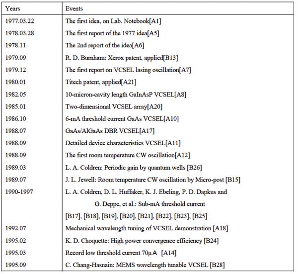
A couple of months later, in May 1995, Yang in Dapkus’s group of University of Southern California, Los Angels, published a paper claiming a lower threshold current of a VCSEL, less than 10 µA[B21]. This data, however, has not been reproduced until this moment. Besides the organizations described here, many others have participated in the research on VCSELs and achieved low threshold current of sub-milliamperes, which include University of Ulm [B22, B23], and Sandia National Laboratories [B24]. In addition to the threshold current reduction of VCSELs described in TableⅠ I and Fig. 11, important and turning innovations led by Kenichi Iga and his team are listed in Table II with significant related achievement by other groups.
(iii) Wavelength-tunable VCSEL
Wavelength/Frequency-tunable VCSELs are important light sources for spectroscopic sensing and datacom with wavelength division multiplexing. A tunable VCSEL was reported for a ranging sensor in combination with a monolithically integrated light beam deflector where the emitting beam angle depends on the wavelength [B3]. Continuous-tuning of 18 Å was achieved by current injection through a newly added electrode into the n-DBR mirror, as reported by Chang-Hasnain et al., of Bellcore, in 1991 [B27]. The active junction can be cooled owing to the Peltier effect or heated by DBR resistance. Another approach toward the continuous frequency-tuning was realized by providing a top DBR mesa and the third electrode into a VCSEL. Highly resistive heterointerfaces of the top DBR mesa cause extra heating of the cavity, resulting in a continuous wavelength change toward the longer wavelength. A wavelength shift of 2.2 nm was derived by the tuning current of 700 μA, as reported by Wipiejewski in Ebeling’s group, at University of Ulm [B22].
To further expand the tunability, Iga’s team verified the wide wavelength tuning (> 40 Å) in a VCSEL with a mechanical movable external mirror[A18], [A19]. Chang-Hasnain of Stanford University realized a monolithic MEMS version of the external mirror VCSEL and showed the record-high wavelength tuning range of 15 nm [B28]. The wavelength tunable VCSEL has opened various applications.
(3) Application Progress of VCSEL in the 21st century
Application areas of VCSEL have been expanding since the late-1990s. They started from short-reach data communications including local area networks (LANs) and optical interconnects inside high-performance computers, servers, and data centers, followed by laser printers, computer mice, displays, and ranging sensors, as shown in Fig. 9 [A2], [A3], [A22], [A23].
(i) LANs and datacom
In response to the rapid growth of internet traffic, strong requirements occurred to expand the network bandwidth in a data center and between data centers. Standardization was promoted in a family of 100 Gbps Ethernet (100 GbE), including 1 00GBASE-SR10, 100GBASE-LR4, and 100GBASE-ER4. SR10 is based on 10 parallel 850-nm multi-mode fiber transmissions with 10 Gbps per fiber. The SR10 supports reaches up to at least 100 m. LR4 and ER4 are based on dense wavelength division multiplexing (DWDM) technology. They support single-mode fiber transmission of at least 10 km and 40 km, respectively. Four wavelength light signals of around 1300 nm with a separation of 800 GHz are transmitted through a single-mode fiber. Each wavelength carries 25 Gb/s. SR10 is supposed to be used in a data center, while ER4 is suitable for connection between data centers. LR4 is applicable to both inside a data center and in-between them; 850-nm VCSELs are supposed to be applied to SR10. For LR4 and ER4, the optional usage of VCSELs and edge-emitting DFB lasers is supposed. For even higher capacity systems, standardization of 400 Gb/s Ethernet was prepared [B29]. In parallel with the effort for the standardization of datacom, such as 100GbEs, research and development are being continuously conducted on optical communication to meet the strong demand for the higher bandwidth.
(ii) Optical interconnects
The main market for VCSELs is, besides the communications for intra- as well as inter-data centers, interconnections in high-performance computers (HPCs) and servers. High-density and highly parallel optical interconnects are extensively deployed for rack-to-rack connections in HPC and servers with multi-mode optical fibers. Requirements for the number of parallel channels and the transmitter/receiver bandwidth are gradually increasing. IBM developed VCSEL-based optical interconnects; 48-channel parallel optical transceivers were demonstrated to transmit and receive up to 20 Gb/s per channel by flip-chip bonding of two optoelectronic arrays with 2 x 12 850 nm VCSEL arrays and GaAs PD arrays on a holey CMOS IC [B30].
Tokyo Institute of Technology announced the start of the operation of a newly developed supercomputer Tsubame 3.0, a leading cloud-type green super computer with high performance and efficient power consumption, where high-capacity and high-speed optical networks connect many computing nodes. The total communication capacity counts 432 Tb/s in the bi-direction mode, whose main body is carried by optical interconnects. The detail is presented on the Web pages of Tokyo Institute of Technology Global Scientific Information and Computer Center [B31].
Effort to increase the modulation bandwidth of VCSELs enabled 64 Gb/s-57m multi-mode optical fiber transmission, as presented by Kuchta of IBM-T. J. Watson Research Center and by Westbergh of Chalmers University of Technology [B32]. Besides such efforts to increase the bandwidth of single-channel, parallel schemes, such as 1 x n or two-dimensional arrangement, m x n, will be indispensable to meet the required aggregate bandwidth. VCSELs are the only solution from the viewpoint of the two-dimensional array configuration and low power-consumption capability. In 2014, aggregated capacity as high as 1.34 Tb/s was realized for incorporation with 2D VCSEL arrays of 14 x 12, as reported by Grabherr and Ebeling of Philips Technologies GmbH U-L-M Photonics, Germany [B33]. A prediction indicated that billions of channels per year will be required soon, as pointed out by Grabherr of Philips GmbH, U-L-M Photonics, Germany [B34]. VCSEL has grown up to be a key component that supports networks and computers of the present and future days.
(iii) Laser printers
A laser printer is known as a high-quality and high-speed machine for digital printing markets. A conventional laser printer often uses a one-dimensional array of lasers, where scanning the laser beams by rotating a polygon mirror. Replacing the one-dimensional laser array with a two-dimensional array of VCSELs, a higher speed of printing is possible while maintaining high printing quality. For example, Fuji Xerox Co. Ltd. developed a high-performance laser raster output scanner using an 8 x 4 VCSEL array as the engine for the printing machine. High quality of 2,400 DPI was achieved with a printing speed of more than 100 sheets per minute by Fuji Xerox Corp. [B35]. The high quality and high-speed operation were realized by applying two-dimensional VCSEL arrays for the first time. Ricoh Co. Ltd. developed a high light-output-power 780 nm array of 40ch VCSELs. By designing and fabricating a low-thermal-resistance DBR mirror, they realized a single-mode light output power of >1.5 mW with reduced thermal interference between VCSELs in the arrays [B36]. With this high-power stable VCSEL array as a multibeam light source, Ricoh Co. Ltd. also produced a high-speed of 150 pages per minute and high precision of 4,800 DPI printing machines [B37].
(iv) Computer mice
The first volume commercial application of VCSELs might be a light source for a computer mouse pointer. The laser mice emerged in 2004. Since then, the shipped quantities of VCSELs have dominated for use in laser mice. Because of the circular output light beam with a small diameter from a single-mode VCSEL, higher tracking precision, as well as a lower electric power consumption is possible in VCSEL mice over the conventional LED mice, as reported by Grabherr in 2013 [B38].
(v)Ranging and sensing
Several companies such as Finisar Corp., II-VI, and Philips U-L-M Photonics shipped 100 to 200 million VCSELs per year in 2013 or 2014, as described by Grabherr in the SPIE Journal referred above[B33]. The total number of VCSELs shipped over the last 20 years is estimated to be nearly 1 billion by Tatum of Finisar Corp. [B39]. Although the past and the present markets, related to VCSEL applications, are still datacom, new and promising volume applications have recently emerged in consumer electronics. They are smart sensors in electronic devices, as described also by Grabherr in the same SPIE journal [B39]. Smartphones today are installed with many VCSELs for use in, for example, laser autofocusing and proximity sensing by time-of-flight range detection, 3D (three dimensional) face recognition for a new security system of smartphones by the use of structured light, low noise optical microphone, and some devices for gesture recognition. These applications will provide a huge potential for VCSEL markets. VCSELs are the most suitable light sources for these applications because of their advantageous features such as low cost owing to high productivity, high reliability, low power consumption, and small size. Fumio Koyama of Tokyo Institute of Technology has succeeded to extend the ranging distance further by monolithic integration of a VCSEL and a VCSEL-based fully solid-state light beam steering device, resulting in a beam steering LiDAR (Light Detection And Ranging) with small size, high resolution, and long measurable distance [B3]. These features are attractive for various sensor applications such as automatic driving, automatic production lines, infrastructure inspection, and many others.
(vi) Iga and his team’s contributions
In summary, Iga’s pioneering work in collaboration with his team revealed many disruptive natures of VCSELs and opened new application areas. VCSEL has developed to be a key component for supporting and further developing the information society of the 21st century. From the original conception to the technology development for higher performance and commercialization of VCSELs, Iga and his team’s contribution is quite significant and difficult to be replaced.
Why was the achievement successful and impactful?
Kenichi Iga envisioned an innovative semiconductor laser characterized by a short laser cavity perpendicular to the wafer surface. This groundbreaking invention has had profound impacts to optoelectronics, offering several distinctive advantages, such as low threshold currents, single-frequency operation, circular beams, scalability to large-scale 2D arrays, and cost-effective manufacturing. His team successfully achieved three pivotal milestones: stable single-frequency oscillation, monolithic fabrication, and continuous frequency tuning. VCSELs have since become integral to modern life, finding widespread applications in LANs, datacenters, 3D face recognition, laser printers, and LiDAR systems.
Supporting texts and citations to establish the dates, location, and importance of the achievement: Minimum of five (5), but as many as needed to support the milestone, such as patents, contemporary newspaper articles, journal articles, or chapters in scholarly books. 'Scholarly' is defined as peer-reviewed, with references, and published. You must supply the texts or excerpts themselves, not just the references. At least one of the references must be from a scholarly book or journal article. All supporting materials must be in English, or accompanied by an English translation.
A: References related directly to the work by Kenichi Iga and his team
[A1] K. Iga, Laboratory Notebook of Precision & Intelligence Laboratory, 1977 Issue, Tokyo Institute of Technology, Tokyo, Japan, Mar. 22, 1977.
[A2] K. Iga, “Forty years of vertical-cavity surface-emitting laser: Invention and innovation”, Jan. J. Appl. Phys., Vol. 57, No. 08PA-1, pp. 1-7, 2018.
[A3] K. Iga, “VCSEL: born small and grown big, “Proc. of SPIE, Vol. 11263, pp. 1126302-1-1126302-13, March 2020.
[A4] K. Iga, and Y. Takahashi, “An Analysis on Single Wavelength Oscillation of Semiconductor Laser at High Speed Pulse Modulation,” Trans. IECE Japan, Vol. E61, No. 9, pp. 68-72, Sept. 1978.
[A5] K. Iga, T. Kambayashi and C. Kitahara, “GaInAsP/InP Surface Emitting Laser(I),” The 25th Spring Meeting of Applied Physics Societies, 27p-C-11, p.63, Mar. 1978 (In Japanese:Translated English text attached).
[A6] C. Kitahara, T. Kambayashi and K. Iga, "GaInAsP/InP Surface Emitting Laser(II)," The 39th Fall Meeting of Applied Phys. Societies, 5p-Z-1, p.497, Nov.,1978. (In Japanese:Translated English text attached).
[A7] H. Soda, K. Iga, C. Kitahara and Y. Suematsu, “GaInAsP/InP Surface-Emitting Injection Lasers,” Jpn. J. Appl. Phys., vol. 18, no. 12, pp. 2329-2330, Dec. 1979.
[A8] Y. Motegi, H. Soda, and K. Iga, “Surface-Emitting GaInAsP/InP Injection Laser with Short Cavity Length,” Electron. Lett., Vol. 18, No. 11, pp. 461-463, May 1982
[A9] K. Iga, S. Kinoshita, and F. Koyama, “Micro-cavity GaAlAs/GaAs Surface-Emitting laser with Ith=6 mA,” International Semiconductor Laser Conference, PD-4, Oct. 1986.
[A10] K. Iga, S. Kinoshita, and F. Koyama, “Micro-cavity GaAlAs/GaAs Surface-Emitting laser with Ith=6 mA,” Electron. Letters, Vol. 23, No. 3, pp. 134-136, 29th, Jan. 1987.
[A11] K. Iga, F. Koyama, and S. Kinoshita, “Surface Emitting Semiconductor Lasers,” IEEE J. Quantum Electronics, Vol. 24, No. 9, pp. 1845-1855, Sept. 1988.
[A12] F. Koyama, S. Kinoshita and K. Iga, “Room temperature CW Operation of GaAs Vertical Cavity Surface Emitting Laser,” Trans. IEICE, Vol. E71, No. 11, pp. 1089-1090, Nov. 1988.
[A13] T. Baba, Y. Yogo, K. Suzuki, F. Koyama and K. Iga, “First Room Temperature CW Operation of GaInAsP/InP Surface Emitting Laser,” IEICE Trans. Electron., Vol. E76-C, No. 9, pp. 1423-1424, Sept. 1993.
[A14] Y. Hayashi, T. Mukaihara, N. Hatori, N. Ohnoki, A. Matsutani, F. Koyama, and K. Iga, “Record low-threshold Index-guided InGaAs/GaAlAs vertical-cavity surface-emitting laser with a native oxide confinement structure,” Electron. Lett., Vol. 31, No. 7, pp. 560-562, Mar. 1995.
[A15] H. Uenohara, F. Koyama, T. Sakaguchi, and K. Iga: “Multi quantum well structure for surface emitting lasers”, National Conference Record, Semiconductor Devices and Materials, IEICE, No. 279, Nov. 1987. (In Japanese: Translated English text attached)
[A16] H. Uenohara, F. Koyama, and K. Iga: “Application of the multi-quantum well (MQW) to a surface emitting laser”, Jpn. J. Appl. Phys., Vol. 28, No. 4, pp. 740-741, April 1989.
[A17] T. Sakaguchi, F. Koyama, and K. Iga, "Vertical Cavity Surface-Emitting Laser with an AlGaAs/AlAs Bragg Reflector," Electron. Lett., Vol. 24, No. 15, pp. 928-929, July 1988.
[A18] N. Yokouchi, T. Miyamoto, T, Uchida, Y, Inaba, F. Koyama, and K. Iga, "40Å continuous tuning of a GaInAsP/InP vertical-cavity surface-emitting laser using an external mirror," IEEE Photon. Technol. Lett., Vol. 4, No. 7, pp. 701-703, July 1992.
[A19] N. Yokouchi, T. Miyamoto, T. Uchida, Y. Inaba, F. Koyama, and K. Iga, “GaInAsP/InP Surface Emitting Laser Grown by CBE and Wavelength Tuning Employing External Reflector,” Int. Conf. on Solid State Devices and Materials, B-6-4, pp. 613-615, Tsukuba, Aug. 1992
[A20] S. Uchiyama and K. Iga, “Two-Dimensional Array of GaInAsP/InP Surface-Emitting Lasers”, Electronics Letters, Vol. 21, No. 4, pp. 162-164, Feb. 1985
[A21] K. Iga, Y. Suematsu, K. Kishino, and H. Soda, ”Surface-Emitting Semiconductor Lasers”, Japanese Patent, applied on January 9th, 1980, and granted as Heisei-1-56547 on November 30th, 1989. (In Japanese: A part of the first page of the patent was translated)
[A22] K. Iga, “Surface emitting laser - Its birth and generation of new optoelectronics field”, IEEE J. Selected Topics in Quantum Electron., Vol.6, No.6, pp.1201-1215, Nov./Dec. 2000
[A23] K. Iga, “Vertical-Cavity Surface-Emitting Laser(VCSEL)”, Proc. IEEE, Vol. 101, No. 10, pp. 2229-2233, Oct. 2013.
[A24] T. Mukaihara, Y. Hayashi, N. Hatori, N. Ohnoki, A. Matsutani, F. Koyama, and K. Iga, “Low-threshold mesa-etched vertical-cavity InGaAs/GaAs surface emitting lasers grown by MOCVD,” Electron. Lett., Vol. 31, No. 8, pp. 647-648, April 1995.
B: References related to work done by teams other than Kenichi Iga.
[B1] Y. Arakawa, and H. Sakaki, “Multidimensional quantum well laser and temperature dependence of its threshold current”, Appl. Phys. Lett., Vol. 40, pp. 939-941, 1982.
[B2] M. Asada, Y. Miyamoto, and Y. Suematsu, “Gain and the threshold of three-dimensional quantum-box lasers”, IEEE J. Quantum Electron., Vol. QE-22, pp. 1915-1921, 1986.
[B3] Z. Ho, K. Shimura, X. Gu, M. Nakahama, A. Matsutani, and F. Koyama, “High-resolution of Beam Steering of Slow Light VCSEL Amplifier”, The 12th Conference of Lasers and Electro-Optics Pacific Rim, 2-1G-5, Aug. 2017.
[B4] I. Melngailis, R. J. Phelan, and R. H. Rediker, “Luminescence and coherent emission in a large-volume injection plasma in InSb,” Appl. Phys. Lett., vol. 5, No. 5, pp. 99-100, Sept. 1964.
[B5] I. Melngailis, “Longitudinal injection-plasma laser of InSb,” Appl. Phys. Lett., Vol. 6, No. 3, pp. 59-60, Feb. 1965.
[B6] G. E. Stillman, M. D. Sirkis, J. A. Rossi, M. R. Johnson, and N. Holonyak Jr., “Volume Excitation of an Ultrathin Single-Mode CdSe Laser”, Appl. Phys. Letts., Vol. 9, pp. 268-269, Oct. 1966.
[B7] N. G. Basov, O. V. Bogdankevich, and A. Z. Grasyuk, “Semiconductor Lasers with Radiating Mirrors”, IEEE J. Quantum Electron., Vol. QE-2, pp. 594-597, September 1966.
[B8] J. R. Packard, W. C. Tait, D. A. Campbell, “Standing Waves and Single-Mode Room-Temperature Laser Emission from Electron-Beam-Pumped Cadmium Sulfide”, IEEE J. Quantum Electron., Vol. QE-5, pp. 44-47, Jan. 1969.
[B9] V. N. Smiley, H. F. Taylor, and A. L. Lewis, “Laser Emission in Thin Dielectric-Coated CdSe Lasers”, J. Appl. Phys., Vol. 42, No. 13, pp. 5859-5861, Dec. 1971.
[B10] H. M. Gibbs, S. L. McCall, T. N. C. Venkatesan, A. C. Gossard, A. Passner, and W. Wiegmann, “Optical Bistability in Semiconductors”, Appl. Phys. Letts., Vol. 35, pp. 451-453, Sept. 15, 1979.
[B11] M. A. Duguay, and T. C. Damen, “Picosecond Pulses from an Optically Pumped Ribbon Whisker Laser”, Appl. Phys. Letts., Vol. 37, p.369-370, Aug. 15, 1980.
[B12] A. Passner, H. M. Gibbs, A. C. Gossard, S. L. McCall, T. N. C. Venkatesan, and W. Wiegmann, “Ultrashort Laser: Lasing in MBE GaAs Layer with Perpendicular-to-Film Optical Excitation and Emission”, IEEE J. Quantum Electron., Vol. QE-16, pp. 1283-1285, Dec. 1980.
[B13] R. D. Burnham, D. R. Scifres, and W. Streifer, applied to US Patent on September 1979, and granted as a patent USP4,309,670, “Transverse Light Emitting Electroluminescent Devices, on January 5th ,1982.
[B14] J. L. Jewell, A. Scherer, S. L. McXll,Y. H. Lee, S. Walker, J. P. Harbison, and L. T. Florez, "Low-Threshold Electrically Pumped Vertical-Cavity Surface-Emitting Microlasers,” Electron. Letts., Vol. 25, pp. 1123-1124, Aug. 1989.
[B15] Y. H. Lee, J. L. Jewell, A. Scherer, S. L. McCall, J. P. Harbison, and L. T. Florex, “Room-Temperature Continuous-Wave Vertical-Cavity Single-Quantum-Well Microlaser Diodes,” Electron. Lett., Vol. 25, No. 25, pp.1377-1378, Sept. 1989.
[B16] D. I. Babic, K. Streubel, R. P. Mirin, J. Pirek, N. M. Margalit, J. E. Bowers, E. L. Hu, D. E. Mars, L. Yang, and K. Carey, “Room temperature performance of double-fused 1.54 micron vertical-cavity lasers,” in IPRM 96, ThA1-2, Apr.1996
[B17]R. S. Geels and L. A. Coldren, “Narrow-Linewidth, Low Threshold Vertical-Cavity Surface-Emitting lasers,” 12th International Semiconductor Laser Conf., Vol. B-1, pp. 16-17, Davos, Switzerland, 9-14 Sept. 1990
[B18] T. Numai, T. Kawakami, T. Yoshikawa, M. Sugimoto, Y. Sugimoto, H. Yokoyama, K. Kasahara, and K. Asakawa, “Record Low Threshold Current in Microcavity Surface-Emitting Laser,” Jpn. J. Appl. Phys, Vol. 32, Part2, No. 10B, pp. L1533-L1534, Oct. 1993
[B19] D. L. Huffaker, D. G. Deppe, K. Kumar, and T. J. Rogers, “Native-oxide defined ring contact for low threshold vertical-cavity lasers,” Appl. Phys. Lett., Vol. 65, No. 1, pp. 97-99, July 1994
[B20] D. L. Huffaker, J. Shin, and D. G. Deppe, “Low threshold half-wave vertical-cavity lasers,” Electron. Lett., Vol. 30, No. 23, pp. 1946-1947, Nov. 1994.
[B21] G. M. Yang, M. H. MacDougal and P. D. Dapkus, “Ultralow threshold current vertical-cavity surface-emitting lasers obtained with selective oxidation,” Electron. Lett., Vol. 31, No. 11, pp. 886-888, May 1995.
[B22l T. Wipiejewski, K. Panzlaf, E. Zeeb, and K. J. Ebeling, “Submilliamp vertical cavity laser diode structure with 2.2-nm continuous tuning,” 18th European Conf. Opt. Comm., PDII-4, Sept.1992.
[B23] M. Grabherr, R. Michalzik, B. Weigl, G. Reiner, and K. J. Ebeling, "Efficient Single-Mode Oxide-Confined GaAs VCSEL's Emitting 850-nm Wavelength Regime," IEEE Photon. Tech. Lett., Vol. 9, No. 10, pp. 1304-1306, Oct. 1997.
[B24] K. L. Lear, K. D. Choquette, R. P. Schneider, Jr., S. P. Kilcoyne and K. M. Geib, “Selectively oxidized vertical cavity surface emitting lasers with 50% power conversion efficiency,” Electron. Lett., Vol. 31, No. 3, pp. 208-209, Feb. 1995.
[B25]J. Ko, R. Hegblom, Y. Akulova, B. J. Thibeault, and L. A. Coldren, “Low-Threshold 840-nm Laterally Oxidized Vertical-Cavity Lasers Using AlInGaAs-AlGaAs Strained Active Layers,” IEEE Photonics Tech. Lett., Vol.9, No. 7, pp. 863-865, July 1997
[B26] S. W. Corzine, R. S. Geels, R. H. Yan, J. W. Scott, and L. A. Coldren: “Efficient, narrow-linewidth distributed-Bragg reflector surface emitting laser with periodic gain,” Photo. Tech. Lett., vol. 1, no. 3, pp. 52-54, March 1989.
[B27] C. J. Chang-Hasnain, J. P. Harbison, C. E. Zah, L. T. Florez, N. C. Andreadakis: "Continuous wavelength tuning of two-electrode vertical cavity surface emitting lasers", Electron. Lett., vol. 27, pp.1002-1003, May 1991.
[B28] M. S. Wu, E. C. Vail, G. S. Li, W. Yuen and C. J. Chang-Hasnain, “Tunable Micromachined Vertical Cavity Surface emitting lasers,” Electron. Lett., Vol. 31, No. 19, pp. 1671-1672, Sept. 1995.
[B29] J. D’ambrosia, “100 Gbit Ethernet and Beyond,” IEEE Communication Magazine, Vol. 48, Issue 3, pp. S6-S13, Mar. 2010.
[B30]F. E. Doany, B. G. Lee, D. M. Kuchta, A. V. Rylakov, C. Baks, C. Jahnes, F. Libsch, and C. L. Schow, “Terabit/Sec VCSEL-Based 48-Channel Optical Module Based on Holey CMOS Transceiver IC”, J. Lightwave Tech., Vol. 31, No. 4, pp. 672-680, Feb. 2013.
[B31] Tsubame 2.5,3.0, please refer web pages. http://www.gsic.titech.jp/en
[B32] D. M. Kuchta, A. V. Rylyakov, C. L. Schow, J. E. Proesel, C. Bals. P. Westbergh, J. S. Gustavsson, and A. Larsson, “64Gb/s Transmission over 57m MMF using an NRZ Modulated 850nm VCSEL,” OFC2014, Th3C.2, March 2014.
[B33] M. Grabherr, S. Intemann, R. King,”VCSEL arrays for high-aggregate bandwidth of up to 1.34 Tbps,” Proc. SPIE 9001, Vertical-Cavity Surface-Emitting Lasers XVIII, 900105, pp. 4-1 to 4-10, Feb. 2014.
[B34] M. Grabherr, “New applications boost VCSEL quantities: recent developments at Philips”, Vertical-Cavity Surface-Emitting Lasers XIX, edited by Chun Lei, and Kent D. Choquette, Proc. of SPIE, Vol. 9381, 938102-1-938102-13, 2015.
[B35] N. Ueki, J. Ichikawa, C. Ikeda, H. Tezuka and A. Ohta, “Light Exposure System Using a Vertical-Cavity Surface-Emitting Laser Diode Array”, Fuji Xerox Tech. Report, No. 16, pp. 11-19. 2006.(in Japanese).
[B36] K. Harasaka, H. Motomura, K. Hara, A. Ito, N. Jikutani, and S. Sato, “Low thermal resistance 780nm GaInPAs/GaInP 40ch VCSEL array for laser printers”, 17th Microoptics Conf.(MOC’11), Sendai, Japan, Paper L2,Oct.- Nov. 2011.
[B37] S. Sato, “Laser printer applications of VCSEL arrays and trends of VCSELs”, Optonews, Vol. 12, No. 1, pp.2-6, 2017. (in Japanese)
[B38] M. Grabherr, H. Moench, and A. Pruijmboon, “VCSELs for Optical Mice and Sensing”, Book of Springer Series in Optical Sciences, October 2013.
[B39] J. A. Tatum, “Evolution of VCSELs”, Proc. Vol. 9001, Vertical-Cavity Surface-Emitting Lasers XVIII, Feb. 2014.
Supporting materials (supported formats: GIF, JPEG, PNG, PDF, DOC): All supporting materials must be in English, or if not in English, accompanied by an English translation. You must supply the texts or excerpts themselves, not just the references. For documents that are copyright-encumbered, or which you do not have rights to post, email the documents themselves to ieee-history@ieee.org. Please see the Milestone Program Guidelines for more information.
Please email a jpeg or PDF a letter in English, or with English translation, from the site owner(s) giving permission to place IEEE milestone plaque on the property, and a letter (or forwarded email) from the appropriate Section Chair supporting the Milestone application to ieee-history@ieee.org with the subject line "Attention: Milestone Administrator." Note that there are multiple texts of the letter depending on whether an IEEE organizational unit other than the section will be paying for the plaque(s).
Please recommend reviewers by emailing their names and email addresses to ieee-history@ieee.org. Please include the docket number and brief title of your proposal in the subject line of all emails.
