Milestone-Proposal:Realization of Blue Light Emitting Diode, 1989-1993
To see comments, or add a comment to this discussion, click here.
Docket #:2024-32
This proposal has been submitted for review.
To the proposer’s knowledge, is this achievement subject to litigation? No
Is the achievement you are proposing more than 25 years old? Yes
Is the achievement you are proposing within IEEE’s designated fields as defined by IEEE Bylaw I-104.11, namely: Engineering, Computer Sciences and Information Technology, Physical Sciences, Biological and Medical Sciences, Mathematics, Technical Communications, Education, Management, and Law and Policy. Yes
Did the achievement provide a meaningful benefit for humanity? Yes
Was it of at least regional importance? Yes
Has an IEEE Organizational Unit agreed to pay for the milestone plaque(s)? Yes
Has the IEEE Section(s) in which the plaque(s) will be located agreed to arrange the dedication ceremony? Yes
Has the IEEE Section in which the milestone is located agreed to take responsibility for the plaque after it is dedicated? Yes
Has the owner of the site agreed to have it designated as an IEEE Milestone? Yes
Year or range of years in which the achievement occurred:
1989-1993
Title of the proposed milestone:
Practical Blue Light-Emitting Diode, 1989–1993
Plaque citation summarizing the achievement and its significance; if personal name(s) are included, such name(s) must follow the achievement itself in the citation wording: Text absolutely limited by plaque dimensions to 70 words; 60 is preferable for aesthetic reasons.
In 1989, the first p-n homo-junction UV light-emitting diodes (LEDs) fabricated using gallium nitride (GaN) were demonstrated by Isamu Akasaki and Hiroshi Amano. In 1993, a blue LED that was 1000 times brighter than earlier works using indium gallium nitride (InGaN) double-heterostructure was first demonstrated by Shuji Nakamura. The result of their combined efforts, recognized by the 2014 Nobel Prize in Physics, transformed lighting and electronics worldwide.
200-250 word abstract describing the significance of the technical achievement being proposed, the person(s) involved, historical context, humanitarian and social impact, as well as any possible controversies the advocate might need to review.
Red and green light-emitting diodes (LEDs), which emit the long wavelengths of visible light were invented rather early, red LEDs in 1962 and green LEDs in 1958. However, proper semiconductor material for blue LEDs had not been found until the innovations in this milestone arrived.
The basic structure of blue LEDs is a p-n junction, and the principle of light emission through the recombination of electrons in conduction band and holes in valence band is the same as for other LEDs. The realization of blue LEDs involved many challenges, including selecting a material with a large band gap width necessary to emit blue light, achieving high-quality crystal growth, realizing p-n junctions, and issues involved in mass production.
In 1989, Isamu Akasaki and Hiroshi Amano achieved the crystal growth and p-n junction of gallium nitride (GaN), which is suitable for blue LEDs. In 1993, Shuji Nakamura realized a high-brightness blue LED, that led to mass production.
Blue LEDs are used in many fields such as lighting and have significantly contributed to the expansion of various industries. For this achievement, the three were awarded the Nobel Prize in Physics in 2014.
The realization of blue LEDs has enabled energy savings, long service life, and high-quality lighting, significantly impacted the advancement of medical technology and expanded the whole industry sector. This innovation distinguishes itself from other blue light-emitting technologies, such as electroluminescence and blue lasers.
IEEE technical societies and technical councils within whose fields of interest the Milestone proposal resides.
IEEE Consumer Technology Society, IEEE Electron Devices Society
In what IEEE section(s) does it reside?
IEEE Nagoya Section
IEEE Organizational Unit(s) which have agreed to sponsor the Milestone:
IEEE Organizational Unit(s) paying for milestone plaque(s):
Unit: IEEE Nagoya Section
Senior Officer Name: Jun Sato
IEEE Organizational Unit(s) arranging the dedication ceremony:
Unit: IEEE Nagoya section
Senior Officer Name: Jun Sato
IEEE section(s) monitoring the plaque(s):
IEEE Section: IEEE Nagoya Section
IEEE Section Chair name: Jun Sato
Milestone proposer(s):
Proposer name: Chiaki Ishikawa
Proposer email: Proposer's email masked to public
Please note: your email address and contact information will be masked on the website for privacy reasons. Only IEEE History Center Staff will be able to view the email address.
Street address(es) and GPS coordinates in decimal form of the intended milestone plaque site(s):
C-TEFs, Nagoya University, Furo-cho, Chikusa-ku, Nagoya, 464-8601, Japan
GPS Coordinates: 35.1510357,136.9709546,17
Describe briefly the intended site(s) of the milestone plaque(s). The intended site(s) must have a direct connection with the achievement (e.g. where developed, invented, tested, demonstrated, installed, or operated, etc.). A museum where a device or example of the technology is displayed, or the university where the inventor studied, are not, in themselves, sufficient connection for a milestone plaque.
Please give the details of the mounting, i.e. on the outside of the building, in the ground floor entrance hall, on a plinth on the grounds, etc. If visitors to the plaque site will need to go through security, or make an appointment, please give the contact information visitors will need. It is a university research center. It is a comprehensive research facility of the gallium arsenide (GaN), the core of the original blue LED. The facility is the only GaN research center in the world that vertically integrates crystal growth, characterization, device design and processing, and circuitry and systems under-one-roof, and is a new facility that will accelerate research and development.
Are the original buildings extant?
No. But the C-TEFs building near the original building is located on the same Nagoya University campus.
Details of the plaque mounting:
The plaque will be displayed in the entrance hall of C-TEFs building, Nagoya University.
How is the site protected/secured, and in what ways is it accessible to the public?
The plaque will be fixed on the wall of entrance hall in C-TEFs building, Nagoya University, which is accessible to the public with permission.
Who is the present owner of the site(s)?
Hiroshi Amano
What is the historical significance of the work (its technological, scientific, or social importance)? If personal names are included in citation, include detailed support at the end of this section preceded by "Justification for Inclusion of Name(s)". (see section 6 of Milestone Guidelines)
Justification of name in citation
In 1989, Isamu Akasaki and Hiroshi Amano achieved crystal growth and p-n junction of gallium nitride (GaN), suitable for blue light emission. In 1993, Shuji Nakamura realized a high-brightness blue light-emitting diode (LED). Blue LEDs are used in many fields, such as lighting, and have significantly contributed to the expansion of various industries. For this achievement, the three were awarded the Nobel Prize in Physics in 2014 [18]. The reason for the award was "the invention of a blue LED that enabled a high-brightness, power-saving white light source." This shows that their research has had a tremendous impact on the scientific community and society as a whole.
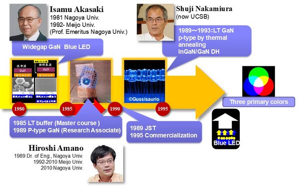
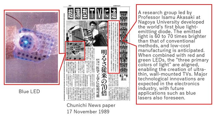
The following figure 1 illustrates the main roles of Akasaki, Amano, and Nakamura. Akasaki had been leading the crystal growth of GaN since around 1980. Since 1982, Amano had been conducting research on GaN crystal growth alongside Akasaki. In 1989, they successfully lit up the first p-n junction blue light-emitting diode. In 1993, Nakamura developed a high-brightness blue LED by inventing the 2-flow method and the double heterojunction of GaN.
Figure 1 The main roles of Isamu Akasaki, Hiroshi Amano, and Shuji Nakamura.
(Source: Reprinted with modifications from the Figure created by Amano with his permission)
Advances in science and technology: The invention of blue LEDs has led
to breakthroughs not only in lighting technology but also in many
fields such as medicine, communications, and electronics. Given such a
wide range of influences, inscribing their names on plaques is
necessary to convey their historical significance to future
generations.
For students and young researchers, their names become a symbol of passion and dedication to the development of science and technology. It is hoped that leaving their names on the plaque will inspire the next generation and encourage new inventions and discoveries.
For these reasons, including the names of Isamu Akasaki, Hiroshi Amano, and Shuji Nakamura on the plaque is of great significance in honoring their technical and social contributions.
Historical Significance
Background
Conventional LEDs (red and green) in visible light wavelengths
Before the invention of blue light-emitting diodes (LED), among visible light wavelengths (λ = 380 nm - 760 nm), LEDs existed that emitted long-wavelength red (λ = 630 nm, typical) and green light (λ = 530-540 nm, typical). Red LEDs were invented in 1962 and green LEDs were invented in 1958.
The development of a reliable blue LED was crucial, as it would enable the combination of red, green, and blue light to produce white light, thereby opening the door to a wide range of full-color display and lighting applications.
However, despite the early invention of green and red LEDs, there were no LEDs that emitted bright enough blue light.
This was the situation before the inventions in this Milestone were made.
Development following the red LED in 1962 into 1970's
In 1962, Nick Holonyak Jr. invented the first practical visible-spectrum (red) LED while working at General Electric [21]. This pioneering work laid the foundation for the commercialization of LEDs in various applications, including indicator lights and displays.
Following this breakthrough, the 1970s witnessed further advancements. In 1972, M. George Craford, a former graduate student of Holonyak, developed the first yellow LED and significantly enhanced the brightness of red and red-orange LEDs. These improvements expanded the utility of LEDs in electronic devices and signage.
Despite these successes, creating LEDs that could emit blue light remained a formidable challenge for several decades. This challenge was eventually overcome in the early 1990s as described in this MILESTONE application, leading to the high-efficiency blue LEDs that revolutionized lighting technology.
These historical events in LED development highlight the persistent efforts and innovations that paved the way for the versatile and energy-efficient lighting solutions we have today.
Difficulty of blue LED: high-power to be recognized by human eyes
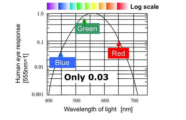
Bright-enough blue LEDs are very difficult to create due to the sensitivity of the human eye, shown in Figure 2. The responsivity of the human eye to pure blue light is only 3% of that to 555 nm yellow-green light. So, for the same brightness recognized by human eyes, blue light should emit 33 times more power than yellow-green light.
Figure 2 Visible light wavelengths
(Source: Reprinted with modifications from the Figure created by Amano with his permission)
Realization of Blue Light Emitting Diode (LED)
Light-Emitting Diode (LED)
The basic structure of a light-emitting diode (LED) is a p-n junction, where a p-type semiconductor (which has many holes) and an n-type semiconductor (which has many electrons) are joined. When a forward voltage is applied to this element, the holes and electrons move toward the p-n junction and recombine, causing the electrons to move from a high-energy state in the conduction band to a low-energy state in the valence band. The energy difference (band gap) between these states is released as light.
Condition for Blue Light Emission
The working principle of blue light emitting diodes (LEDs) is the same
as that of general diodes. They emit light when electrons recombine
with holes in the p-n junction. The band gap in which the electrons fall into the valence band determines the color emitted.
The band gap (Bg) [eV] and the wavelength (λ) in micrometer [μm] of
the emitted color are approximately related by the following formula.:
λ=1.24/Bg
To emit blue light (λ = 0.46-0.47 μm, typical), a semiconductor with a band gap of about 2.6 eV is required.
The challenges in realizing a blue LED
The basic structure of a blue light-emitting diode (LED) is the same as that of conventional diodes, featuring a p-n junction. The principle of light emission, where electrons in a conductor band emit light by recombining with holes, is also the same as that of ordinary diodes. Therefore, the challenges in realizing a blue LED included:
(a) Creating a crystal with a wide band gap that can emit blue light;
(b) Making high-quality p-n junctions;
(c) Producing a high-brightness light-emitting diode.
The Nobel Prize in Physics [18]
In 1989, Isamu Akasaki and Hiroshi Amano achieved the crystal growth and p-n junction of gallium nitride (GaN), which is suitable for blue light emission. In 1993, Shuji Nakamura realized a high-brightness blue LED. For this achievement, Isamu Akasaki, Hiroshi Amano, and Shuji Nakamura were awarded the Nobel Prize in Physics in 2014 [1]. The reason for the award was "the invention of a blue light emitting diode that enabled a high-brightness, power-saving white light source."
Social Impact of the Realization of Blue Light Emitting Diodes
The realization of blue light-emitting diodes (LEDs) has had numerous social impacts. Here are some examples:
(a) Energy savings: Blue LEDs are very energy efficient compared to traditional incandescent and fluorescent bulbs, resulting in a significant reduction in electricity consumption. This has lessened the environmental burden and promoted sustainable energy use.
(b) Long service life: Blue LEDs have a very long lifespan and need to be replaced infrequently, which reduces maintenance costs. This has alleviated the economic burden and contributed to waste reduction.
(c) High-quality lighting: Blue LEDs have a high color temperature and provide brightness close to natural light. This has improved both the environment and the quality of work, as well as enhanced visual comfort.
(d) Advances in medical technology: Blue LEDs are also being utilized in the medical field. For example, they are used in phototherapy and dental procedures. This has increased the effectiveness of treatments and improved patients' quality of life.
The scale of the blue LED industry is expanding year by year, and further technological innovations and market expansion are expected in the future. Thus, blue LEDs have become an essential technology in many industries.
Figure 3 shows how InGaN LEDs can contribute to improving the electricity supply and demand situation of Japan.
Many people will remember the great earthquake of east Japan and the meltdown of the nuclear power plants in 2011.
Before 2011, about 30% of Japan’s electricity was generated by nuclear reactors.
After 2011, all nuclear plants in Japan have been shut down temporarily.
So, we have to find a way of compensating for the loss of 30% of Japan’s generating capacity.
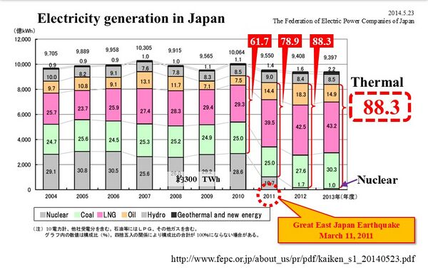
Figure 3 Electricity generation in Japan
(Source: Reprinted with modifications from the Figure created by Amano with his permission)
A research company in Japan predicted, in 2014, that by 2020, 70% of the general lighting systems have been replaced by LED lighting, allowing a 7% reduction in uses, shown in Figure 4.
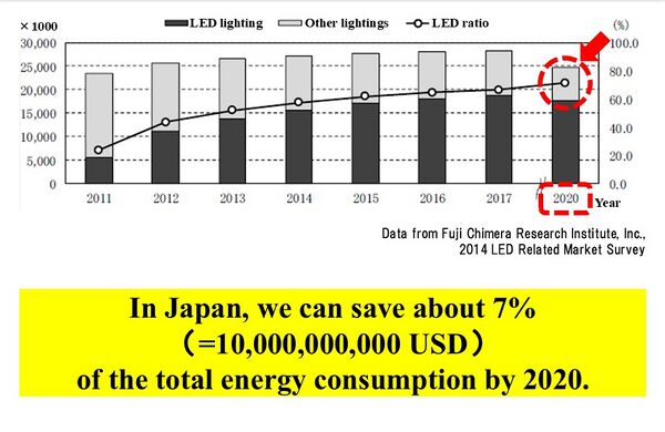
Figure 4 Energy consumption in Japan
(Source: Reprinted with modifications from the Figure created by Amano with his permission)
What obstacles (technical, political, geographic) needed to be overcome?
Obstacles to overcome
There were three challenges in realizing blue LEDs. that is (1) High-quality crystal growth of GaN suitable for blue light emission (2) Realization of P-type GaN (3) Heterostructure semiconductor devices
(1) and (2) correspond to challenges (a) and (b) in "The challenges in realizing
a blue LED".
(3) turned out to be the solution for the challenge (c).
High-quality crystal growth of GaN suitable for blue light emission
Materials for Blue Light Emission
To emit blue light (λ = 450-470 nm, typical value), a semiconductor with a band gap of about 2.6 eV is required. Silicon (Si) with a band gap of 1.2 eV and gallium arsenide (GaAs) with a band gap of 1.4 eV do not meet these requirements due to their narrow band gaps. Therefore, gallium nitride (GaN), zinc selenide (ZnSe), and silicon carbide (SiC) with a wide band gap were considered as candidates for blue light-emitting semiconductors. However, SiC has an indirect band gap and low luminous efficiency. ZnSe has the advantage of having the same atomic spacing as GaAs, and many researchers have tried to make crystals with ZnSe. However, it turned out that ZnSe is not suitable for practical use due to its brittleness. GaN did not have a suitable substrate, and few researchers focused on it. Nonetheless, Akasaki and Amano chose GaN as the material[2], and their pioneering efforts led to major advances in blue LED technology.
Substrate material for GaN
Akasaki and Amano chose sapphire (aluminum oxide, α-Al2O3) as the substrate material for GaN crystal growth [1]. The reason was its affordability, resistance to high temperatures and ammonia, and overall durability. Initially, they faced difficulties in growing GaN on sapphire substrates. They first looked at the halogen vapor deposition (HVPE) method and made a number of improvements to the reaction tube and substrate. However, it turned out that temperature control was difficult with this method. Subsequently, Akasaki switched to metal-organic vapor deposition (MOVPE) and succeeded in growing GaN crystals [3].
Crystal Growth of GaN
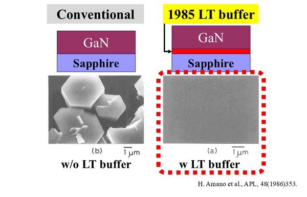
Sapphire and GaN have different crystal structures, and the atomic spacing is 16% different. As a result, clean GaN crystal growth on sapphire substrates was initially not possible. Therefore, Amano devised a low-temperature buffer layer in which aluminum nitride (AlN) impurities are sandwiched between the sapphire substrate and GaN [5], [17]. Amano thought that AlN could be used to effectively grow GaN with better surface morphology. At one point, due to a malfunction of the equipment, he was unable to bring the epitaxial temperature of AlN to the original set temperature of 1200°C. He stopped to ponder and theorized that if AlN is supplied in small quantities at low temperatures, AlN will function as a nucleation center and promote the growth of AIN. Then, as expected, he created a thin buffer layer of AlN, and succeeded in forming GaN crystals on top of that layer.
Figure 5 a thin buffer layer of AlN (Source: Reprinted with modifications from the Figure created by Amano with his permission)
He tried to check the surface using a differential interference contrast microscope of the Nomarsky type. He found that he succeeded in growing flat GaN at the atomic level, as shown in Figure 5. In response to Prof. Akasaki's suggestion, Amano also checked other qualities such as crystallinity, optical and electrical properties, all of which were superior to previous reports. Such a buffer layer is now called a low-temperature buffer layer and is used by many researchers around the world. This technique was patented as US37872724. [P1]
Subsequently, Nakamura developed a low-temperature buffer layer technology using GaN instead of AlN [6], [8].
Realization of p-type GaN crystals
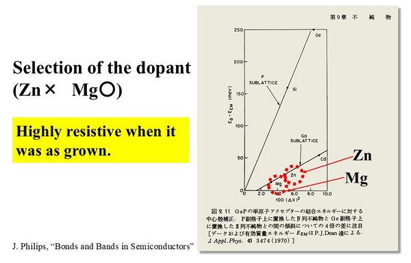
As a general rule, GaN-based semiconductor is n-type. To create a p-n junction diode, p-type GaN must be grown on this n-type GaN base. The use of zinc (Zn) as a dopant to create p-type GaN had been a common practice. However, this approach was not successful. When Amano read the textbook "Bonds and Bands in Semiconductors" written by Dr. Phillips [20] , he learned that Mg was superior to Zn in the activation of acceptors.
Figure 7 Mg was superior to Zn in the activation of acceptors (Source: Reprinted with modifications from the Figure created by Amano with his permission)
Therefore, Amano examined the use of magnesium (Mg), which had not been attempted as a GaN dopant so far. Amano discovered a phenomenon called low-energy electron beam irradiation (LEEBI), in which cathodoluminescence becomes stronger when Mg-doped GaN is irradiated with an electron beam. Hot probing measurements were performed after LEEBI treatment, and p-type behavior was observed in some samples. So, he measured the Hall effect of that sample. Finally, Akasaki and Amano recognized that they had created p-type GaN.
Next, they fabricated a pn-junction LED. Using the above method, Nakamura succeeded in growing p-type GaN on an n-type GaN substrate [7].
On the other hand, in 1992, Nakamura et al. elucidated that the mechanism of p-typing is essentially hydrogen desorption, that is, the Mg acceptor is inactivated by hydrogen immediately after growth. In addition, a method for activating Mg by simple heat treatment was proposed, and p-type GaN was realized accordingly [11]. Today, almost all LED manufacturers use this technology.
Heterostructure semiconductor device
Semiconductors emitting blue light in the band gap
GaN has a band gap of 3.4 eV, so it emits ultraviolet light. It has a shorter wavelength (λ~0.36 μm) than blue-visible light (λ > 0.38 μm). In other words, Akaike and Amano developed an LED that emits faint blue light in the visible light region, as shown in Fig. 8 [14], [15]. Most of the energy is in the ultraviolet region.
Fig. 8 Blue LEDs of Akasaki and Amano (Source: Reprinted with modifications from the Figure created by Amano with his permission)
Therefore, in order to achieve blue light emission, Akaike and Amano tried the following two approaches to make the transition energy smaller [10].
(i) Mix impurities with a short band gap into the light-emitting layer.
(ii) Design an energy level in which electrons fall from the donor level to the acceptor level, rather than a direct transition from the conduction band to the valence band.
Amano et al. used GaN with a band gap of 3.4 eV mixed with indium nitride (InN) with a band gap of 0.7 eV in the hope of reducing the overall band gap to about 2.6 eV. However, it was difficult to synthesize indium gallium nitride (InGaN) crystals using the high-pressure method known at the time.
Mixed Crystal Growth of InGaN
Nakamura was experimenting with mixed crystal growth of InGaN. At that time, due to the poor flow of gas in the reaction tube of his lab devices, it was difficult to create large mixed crystals of InGaN with a band gap suitable for blue light emission. Nakamura set out to solve the gas flow problem in the reaction tube and devised the "Two Flow MOCVD method" to regulate the gas flow [8], [9]. And he succeeded in growing beautiful mixed crystals of InGaN. This technique was patented as US5334277A. [P2].
Double heterojunction in which InGaN is sandwiched between GaN
In the first half of the 1990s, Akasaki, Amano et al. conducted research on AlGaN/GaN heterostructure LEDs. In a simple pn junction consisting of two layers, the p-type GaN layer alone could not obtain sufficient blue luminescence brightness. This is because GaN tends to emit violet and ultraviolet light due to its band gap size.
On the other hand, Nakamura et al. were conducting research on InGaN/GaN or InGaN/AlGaN. Nakamura et al. achieved great success with InGaN, and as a result, in 1994, they realized an InGaN/AlGaN double heterostructure LED with a quantum efficiency of 2.7% (surprisingly high efficiency at that time) [9]. As a basis for these works, the direction of research and development of high-efficiency blue LEDs was clarified, and the future application possibility of blue LEDs became solid. Nakamura succeeded in growing a GaN layer on a sapphire substrate without forming an AlN layer, and forming a large indium gallium nitride (InGaN) mixed crystal [11], [12]. InGaN had a band gap suitable for emitting blue visible light.
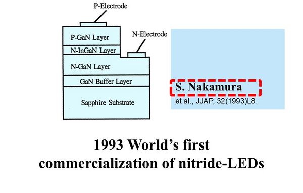
In 1993, Nakamura devised a double heterostructure in which the light-emitting layer of InGaN is sandwiched between two layers of GaN, one p-type and one n-type. Furthermore, he devised a quantum well structure in which p-type GaN and n-type GaN were modified to form a mixed crystal of aluminum gallium nitride (AlGaN) with a large band gap. This development led to the creation of blue light-emitting diodes that emit high-intensity blue light in the InGaN layer [11], [13], [16]. This heterostructure was patented as US5578839A. [P3]
Nakamura's team combined high-quality crystal growth technology, p-type growth technology, and InGaN growth technology to successfully commercialize InGaN blue LEDs for the first time, as shown in Figure 10. In 1995, he also fabricated a single-quantum well LED, which was also a very important technology to increase the efficiency of nitride LEDs.
Figure 10 Commercialization of nitride-LED (Source: Reprinted with modifications from the Figure created by Amano with his permission)
What features set this work apart from similar achievements?
Features that set this work apart from similar achievements
Mechanism to emit blue light
In addition to blue light-emitting diodes (LEDs), there are several other methods to emit blue light. For example, neon signs use blue neon gas, fluorescent lamps and CRTs emit blue light through X-rays and cathode rays using blue phosphors. However, these methods have disadvantages, such as requiring large amounts of power and difficulty in miniaturization.
Furthermore, after the development of blue LEDs, blue lasers were created as an extension of the technology, capable of emitting blue light at specific wavelengths. Additionally, electroluminescence is another phenomenon where certain chemicals emit blue light when an electric current passes through them.
Realization methods of blue light-emitting diode
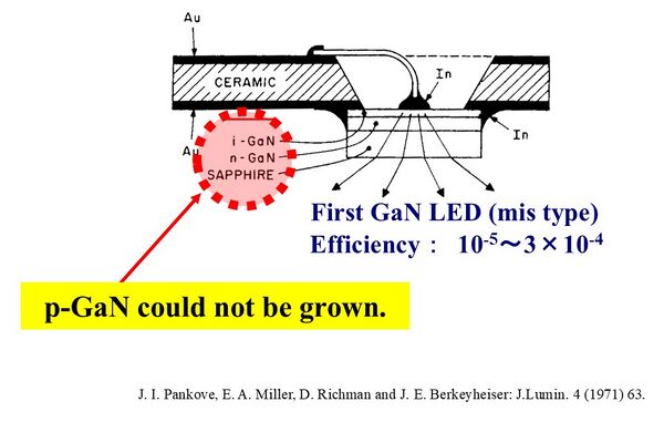
In 1971, Professor Pankove developed the first GaN-based blue LEDs, which was a metal-insulator-semiconductor (MIS) type fabricated by hydride vapor phase epitaxy, one of the thin film growth methods using chemical reaction of Ga and hydrogen chloride and ammonia, shown in Figure 11 [19]. At that time, it was thought to be impossible to grow p-type GaN because of self-compensation. Self-compensation means if we dope acceptor impurity, the same number of intrinsic donors is generated and compensate the doped acceptor.
Figure 11
In 1974, there was a report of a MIS-type blue light-emitting diode that combined metal and semiconductor, differing from p-n junction diodes. However, this method resulted in poor luminous efficiency and insufficient brightness [12].
Why was the achievement successful and impactful?
Why was the achievement successful and impactful?
Here's why it was so successful and impactful:
(a) Technological breakthroughs: The breakthroughs made by Isamu Akasaki, Hiroshi Amano, and Shuji Nakamura shattered the limits of conventional technology. The realization of high-quality crystal growth and p-n junctions using gallium nitride (GaN) and the development of high-brightness blue light-emitting diodes (LEDs) were impossible with previous technologies. This achievement revolutionized lighting technology by enabling the creation of blue LEDs.
(b) Extensive application and social impact: The realization of blue
LEDs has brought numerous benefits, such as increased energy
efficiency, energy savings, long service life, and high-quality
lighting. These advancements have reduced environmental impact,
promoted sustainable energy use, and significantly contributed to the
expansion of various industries. Additionally, blue LEDs have been
applied in diverse fields, including medical technology, communication
technology, and electronics, greatly impacting society as a whole.
(c) Recognition through the Nobel Prize: In 2014, the trio
who contributed to the realization of blue LEDs were awarded the Nobel
Prize in Physics, recognizing their technical achievements and social
impact on an international scale. The award cited "the invention of
the blue light emitting diode, which has enabled bright and
energy-saving white light sources," highlighting the profound impact
their research has had on both the scientific community and society.
For these reasons, the realization of blue LEDs stands as a technological triumph and an achievement with significant social impact.
Supporting texts and citations to establish the dates, location, and importance of the achievement: Minimum of five (5), but as many as needed to support the milestone, such as patents, contemporary newspaper articles, journal articles, or chapters in scholarly books. 'Scholarly' is defined as peer-reviewed, with references, and published. You must supply the texts or excerpts themselves, not just the references. At least one of the references must be from a scholarly book or journal article. All supporting materials must be in English, or accompanied by an English translation.
Bibliography
References
[1] H. Amano, N. Sawaki, I. Akasaki; Y. Toyoda; “Metalorganic vapor phase epitaxial growth of a high quality GaN film using an AlN buffer layer”, Appl. Phys. Lett. 48, pp. 353–355 (1986).
https://doi.org/10.1063/1.96549
https://pubs.aip.org/aip/apl/article-abstract/48/5/353/1023095/Metalorganic-vapor-phase-epitaxial-growth-of-a,
[Abstract]
Atmospheric pressure metalorganic vapor phase epitaxial growth and characterization of high quality GaN on sapphire (0001) substrates are reported. Using AlN buffer layers, GaN thin films with optically flat surfaces free from cracks are successfully grown. The narrowest x‐ray rocking curve from the (0006) plane is 2.70′ and from the (202̄4) plane is 1.86′. Photoluminescence spectra show strong near band edge emission. The growth condition dependence of crystalline quality is also studied.
[2] Hiroshi Amano, Kazumasa Hiramatsu and Isamu Akasaki; “Heteroepitaxial Growth and the Effect of Strain on the Luminescent Properties of GaN Films on (11 bar 20) and (0001) Sapphire Substrates”, Japanese Journal of Applied Physics, Vol. 27, No. 8A, L1384, (1988).
DOI 10.1143/JJAP.27.L1384
https://iopscience.iop.org/article/10.1143/JJAP.27.L1384
[Abstract]
GaN films grown on (11 bar 20) and (0001) sapphire substrates are characterized by X-ray Bond's method and the low temperature photoluminescence measurement. The GaN films are found to be strained by the biaxial compressive stress. From the measured strain and the shift of PL peak energy, the deformation potential of GaN (the relation between the strain parallel to the c-axis and the band gap energy) is found to be 12 eV. The origin of this compressive stress is discussed.
[3] Hiroshi Amano, Isamu Akasaki, Takahiro Kozawa, Kazumasa Hiramatsu, Nobuhiko Sawaki, Kousuke Ikeda, Yoshikazu Ishii; “Electron beam effects on blue luminescence of zinc-doped GaN”, Journal of Luminescence, Vol. 40–41, pp. 121-122, February 1988.
https://doi.org/10.1016/0022-2313(88)90117-2
https://www.sciencedirect.com/science/article/abs/pii/0022231388901172
[Abstract]
9–30kV electron-beam irradiation enhances the blue luminescence in zinc-dop GaN both at low temperature and room temperature. Dependence on irradiation conditions is studied in detail and the mechanism is discussed.
[4] Hiroshi Amano, Masahiro Kito, Kazumasa Hiramatsu and Isamu Akasaki; “P-Type Conduction in Mg-Doped GaN Treated with Low-Energy Electron Beam Irradiation (LEEBI)”, Japanese Journal of Applied Physics, Vol. 28, No. 12A, L2112 (1989).
DOI 10.1143/JJAP.28.L2112
https://iopscience.iop.org/article/10.1143/JJAP.28.L2112/pdf
[Abstract]
Distinct p-type conduction is realized with Mg-doped GaN by the low-energy electron-beam irradiation (LEEBI) treatment, and the properties of the GaN p-n junction LED are reported for the first time. It was found that the LEEBI treatment drastically lowers the resistivity and remarkably enhances the PL efficiency of MOVPE-grown Mg-doped GaN. The Hall effect measurement of this Mg-doped GaN treated with LEEBI at room temperature showed that the hole concentration is ∼2·1016cm-3, the hole mobility is ∼8 cm2/V·s and the resistivity is ∼35 Ω·cm. The p-n junction LED using Mg-doped GaN treated with LEEBI as the p-type material showed strong near-band-edge emission due to the hole injection from the p-layer to the n-layer at room temperature.
[5] Hiroshi Amano, Tsunemori Asahi and Isamu Akasaki; “Stimulated Emission Near Ultraviolet at Room Temperature from a GaN Film Grown on Sapphire by MOVPE Using an AlN Buffer Layer”, Japanese Journal of Applied Physics, Volume 29, Number 2A. L205 (1990).
DOI 10.1143/JJAP.29.L205
https://iopscience.iop.org/article/10.1143/JJAP.29.L205/pdf
[Abstract]
We report the first observation of the room temperature stimulated emission near UV from a GaN film which was grown by metalorganic vapor phase epitaxy on a (0001) sapphire substrate using an AlN buffer layer. This indicates that the GaN film is promising for the realization of an UV laser diode.
[6] Shuji Nakamura; “In Situ Monitoring of GaN Growth Using Interference Effects”, Japanese Journal of Applied Physics, Vol. 30, No. 8R, L1620, (1991).
DOI 10.1143/JJAP.30.1620
https://iopscience.iop.org/article/10.1143/JJAP.30.16207
[Abstract]
The interference effect was observed as an oscillation of the intensity of the transmitted IR radiation through the epitaxial film from the carbon susceptor during GaN growth using an IR radiation thermometer in metalorganic chemical vapor deposition (MOCVD). The IR radiation transmission intensity (IR-RTI) oscillations in GaN growth with and without an AlN buffer layer were studied in detail. The amplitude of the oscillation decreased with increasing thickness due to the thickness fluctuation of the growing GaN film within the measured spot area. In GaN growth with the AlN buffer layer, a very strong oscillation was observed because the surface morphology was much improved by the prior deposition of the AlN buffer layer. The sharp drop of the IR-RTI, which was attributed to the generation of the island growth of GaN around the nucleation site of the AlN buffer layer, was observed at a thickness of about 0.3 µm.
[7] Shuji Nakamura, Masayuki Senoh and Takashi Mukai; “Highly P-Typed Mg-Doped GaN Films Grown with GaN Buffer Layers”, Japanese Journal of Applied Physics, Vol. 30, No. 10A, L1708, (1991).
DOI 10.1143/JJAP.30.L1708
https://iopscience.iop.org/article/10.1143/JJAP.30.L1708/pdf
[Abstract]
Mg-doped GaN films were grown with GaN buffer layers on a sapphire substrate. Hall-effect measurement of as-grown GaN films showed that the hole concentration was 2×10¹⁵/cm3, the hole mobility was 9 cm2/V·s and the resistivity was 320 Ω·cm at room temperature. After the low-energy electron-beam irradiation (LEEBI) treatment, each value became 3×10¹⁸/cm3, 9 cm2/V·s and 0.2 Ω·cm at room temperature, respectively. This value of the hole concentration is the highest ever reported for the p-type GaN films and that of the resistivity is the lowest.
[8] Shuji Nakamura; “GaN Growth Using GaN Buffer Layer”, Japanese Journal of Applied Physics, Vol. 30, No. 10A, L1705, (1991).
DOI 10.1143/JJAP.30.L1705
https://iopscience.iop.org/article/10.1143/JJAP.30.L1705
[Abstract]
High-quality gallium nitride (GaN) film was obtained for the first time using a GaN buffer layer on a sapphire substrate. An optically flat and smooth surface was obtained over a two-inch sapphire substrate. Hall measurement was performed on GaN films grown with a GaN buffer layer as a function of the thickness of the GaN buffer layer. For the GaN film grown with a 200 Å-GaN buffer layer, the carrier concentration and Hall mobility were 4×10¹⁶/cm3 and 600 cm2/V·s, respectively, at room temperature. The values became 8×10¹⁵/cm3 and 1500 cm2/V·s at 77 K, respectively. These values of Hall mobility are the highest ever reported for GaN films. The Hall measurement shows that the optimum thickness of the GaN buffer layer is around 200 Å.
[9] Shuji Nakamura, Takashi Mukai and Masayuki Senoh; “High-Power GaN P-N Junction Blue-Light-Emitting Diodes”, Japanese Journal of Applied Physics, Vol. 30, No. 12A, L1998, (1991).
DOI 10.1143/JJAP.30.L1998
https://iopscience.iop.org/article/10.1143/JJAP.30.L1998/pdf
[Abstract]
High-power p-n junction blue-light-emitting diodes (LEDs) were fabricated using GaN films grown with GaN buffer layers. The external quantum efficiency was as high as 0.18%. Output power was almost 10 times higher than that of conventional 8-mcd SiC blue LEDs. The forward voltage was as low as 4 V at a forward current of 20 mA. This forward voltage is the lowest ever reported for GaN LEDs. The peak wavelength and the full width at half-maximum (FWHM) of GaN LEDs were 430 nm and 55 nm, respectively.
[10] Kenji Itoh, Takeshi Kawamoto, Hiroshi Amano, Kazumasa Hiramatsu Kazumasa Hiramatsu and Isamu Akasaki Isamu Akasaki; “Metalorganic Vapor Phase Epitaxial Growth and Properties of GaN/Al0.1Ga0.9N Layered Structures”, Japanese Journal of Applied Physics, Vol. 30, No.9R, L1924, (1991).
DOI 10.1143/JJAP.30.1924
https://iopscience.iop.org/article/10.1143/JJAP.30.1924
[Abstract]
High-quality, well-controlled GaN/Al0.1Ga0.9N layered structures with periodicity varying from 4.5 nm to 60 nm have been successfully grown on (0001) sapphire substrates by Metalorganic Vapor Phase Epitaxy (MOVPE). The layered structure has been confirmed by double-crystal X-ray diffractometry. Photoluminescence peak energy showed a shift toward the higher-energy side with decreasing thickness of the GaN well layer, which is in good agreement with the calculation obtained from the Kronig-Penny analysis.
[11] Shuji Nakamura, Takashi Mukai, Masayuki Senoh and Naruhito Iwasa; “Thermal Annealing Effects on P-Type Mg-Doped GaN Films”, Japanese Journal of Applied Physics, Vol. 31, No. 2B, L139, (1992).
DOI 10.1143/JJAP.31.L139
https://iopscience.iop.org/article/10.1143/JJAP.31.L139/pdf
[Abstract]
Low-resistivity p-type GaN films were obtained by N2-ambient thermal annealing at temperatures above 700°C for the first time. Before thermal annealing, the resistivity of Mg-doped GaN films was approximately 1×10⁶ Ω·cm. After thermal annealing at temperatures above 700°C, the resistivity, hole carrier concentration and hole mobility became 2 Ω·cm, 3×10¹⁷/cm3 and 10 cm2/V·s, respectively. In photoluminescence measurements, the intensity of 750-nm deep-level emissions (DL emissions) sharply decreased upon thermal annealing at temperatures above 700°C, as did the change in resistivity, and 450-nm blue emissions showed maximum intensity at approximately 700°C of thermal annealing.
[12] Shuji Nakamura, Naruhito Iwasa, Masayuki Senoh and Takashi Mukai; “Hole Compensation Mechanism of P-Type GaN Films”, Japanese Journal of Applied Physics, Vol. 31, No. 5R, L1258, (1992).
DOI 10.1143/JJAP.31.1258
https://iopscience.iop.org/article/10.1143/JJAP.31.1258/pdf
[Abstract]
Low-resistivity p-type GaN films, which were obtained by N2-ambient thermal annealing or low-energy electron-beam irradiation (LEEBI) treatment, showed a resistivity as high as 1×10⁶ Ω·cm after NH3-ambient thermal annealing at temperatures above 600°C. In the case of N2-ambient thermal annealing at temperatures between room temperature and 1000°C, the low-resistivity p-type GaN films showed no change in resistivity, which was almost constant between 2 Ω·cm and 8 Ω·cm. These results indicate that atomic hydrogen produced by NH3 dissociation at temperatures above 400°C is related to the hole compensation mechanism. A hydrogenation process whereby acceptor-H neutral complexes are formed in p-type GaN films was proposed. The formation of acceptor-H neutral complexes causes hole compensation, and deep-level and weak blue emissions in photoluminescence.
[13] Shuji Nakamura, Masayuki Senoh and Takashi Mukai; “P-GaN/N-InGaN/N-GaN Double-Heterostructure Blue-Light-Emitting Diodes”, Japanese Journal of Applied Physics, Vol. 32, No. 1A, L8. (1993)
DOI 10.1143/JJAP.32.L8
https://iopscience.iop.org/article/10.1143/JJAP.32.L8
[Abstract]
P-GaN/n-InGaN/n-GaN double-heterostructure (DH) blue-light-emitting diodes (LEDs) were fabricated successfully for the first time. The output power was 125 µW and the external quantum efficiency was as high as 0.22% at a forward current of 20 mA at room temperature. The peak wavelength and the full width at half-maximum (FWHM) of the electroluminescence (EL) were 440 nm and 180 meV, respectively. This value FWHM of was the smallest ever reported for blue GaN LEDs.
[14] Hiroshi AMANO and Isamu AKASAKI; “GaN blue and UV light emitting diodes with a pn junction”, Japanese Journal of Applied Physics, Vol. 60, No. 2, pp. 163-166, (1991)
(GaN pn 接合青色・紫外発光ダイオード in Japanese)
DOI: https://doi.org/10.11470/oubutsu1932.60.163
Available at: https://www.jstage.jst.go.jp/article/oubutsu1932/60/2/60_2_163/_article/-char/en
[Abstract] (Translated from the original Abstract)
The conductivity control of GaN was investigated. The resistance of the n-type was reduced by Si doping. The resistance of the p-type was increased by Mg doping, and the conductivity was realized for the first time by applying electron beam irradiation to the Mg-doped GaN. We prototyped a pn-junction LED using GaN for the first time, and found that ultraviolet light emission based on interband transitions in the n layer and blue light emission based on the blue emission level involving Mg in the p layer can be used.
[15] Hiroshi AMANO and Isamu AKASAKI; “Present and future prospects
of GaN-based short-wavelength light emitting devices”, Japanese
Journal of Applied Physics, Vol. 63, No. 12, pp. 1243-1247, (1994).
(窒化ガリウム系短波長発光素子の最近の進歩 in Japanese)
https://doi.org/10.11470/oubutsu1932.63.1243
Available online at:
https://www.jstage.jst.go.jp/article/oubutsu1932/63/12/63_12_1243/_article/-char/en
[Abstract] (Translated from the original Japanese abstract)
The success of short-wavelength light-emitting diodes using group III nitrides is as follows: (1) Improvement of the quality of crystals on sapphire by a low-temperature deposition buffer layer, (2) Realization of p-type crystals and p-n junctions, (3) Discovery of impurities that form high-efficiency emission levels, (4) Discovery of the luminescence intensity at the same time as p-forming, and (5) Detection of emission wavelength control by the use of mixed crystals. In this paper, we introduce the history of these technological developments and touch on the future direction of group III nitride research.
[16] Shuji NAKAMURA; “Present status and future prospects of GaN-based light emitting devices”, Japanese Journal of Applied Physics, Vol. 65, No. 7, pp. 676-686, (1995)
(GaN系発光素子の現状と将来 in Japanese)
DOI: https://doi.org/10.11470/oubutsu1932.65.676
Available online at: https://www.jstage.jst.go.jp/article/oubutsu1932/65/7/65_7_676/_article/-char/ja/
[Abstract] (Translated from the original Japanese abstract)
The realization of short-wavelength blue light-emitting devices for
high-intensity full-color lighting diodes (LEDs) or high-density
recording of optical discs such as digital video discs (DVDs) has been
a dream of researchers studying wide band gap semiconductor materials for long-standing purposes. In addition, a blue-violet semiconductor laser with a wavelength of 390~430 nm, which is the shortest wavelength among semiconductor lasers, was also developed for the first time in the world at the end of 1995 by using the InGaN multi-quantum well structure as a light-emitting layer.
[17] Hiroshi AMANO and Isamu AKASAKI; “Effect of low-temperature-deposited layer on the growth of group III nitrides on sapphire”, Japanese Journal of Applied Physics, Vol. 68, No. 7, pp. 768-773, (1999).
(サファイア基板上III族窒化物半導体成長における低温堆積層 in Japanese)
DOI: https://doi.org/10.1380/jsssj.21.126
Available online at: https://www.jstage.jst.go.jp/article/jsssj/21/3/21_3_126/_pdf/-char/en
[Abstract]
Surface control by low-temperature deposited buffer layer enables the growth of high-quality GaN on a sapphire substrate the lattice mismatch of which is as large as 14%. With use of such highly mismatched systems, novel electronic devices such as new lighting source which replaces conventional light bulb, super-high-density optical storage systems, high-power and high-speed transistors and UV image sensors for remote sensing and flame detection will be realized. This paper describes the details of the mechanism of this surface control technology.
[18] The Nobel Prize in Physics 2014
Retrieved 26 December 2024: https://www.nobelprize.org/prizes/physics/2014/summary/
[Remarks] The Nobel Prize in Physics 2014 was awarded jointly to Isamu Akasaki, Hiroshi Amano and Shuji Nakamura "for the invention of efficient blue light emitting diodes which has enabled bright and energy-saving white light sources".
[19] J. P. Pankove and M. A. Lampert; ” Model for Electroluminescence in GaN”, Physical Review Letters, pp. 361-364, Vol. 3, No. 6, 1974
DOI: https://doi.org/10.1103/PhysRevLett.33.361
https://journals.aps.org/prl/abstract/10.1103/PhysRevLett.33.361
[Abstract]
A model to explain dc electroluminescence in GaN diodes is
presented. The voltage applied to the diode is partially localized at
sharp points and ridges at the cathode. Electrons, tunnel-injected
into the active material at the points and ridges, gain sufficient
kinetic energy in the high field to cause impact excitation of the
luminescent center either directly or indirectly (electron-hole-pair
impact excitation across the GaN gap with subsequent hole capture by
the luminescent center).
[20] J. C. Phillips: “Bonds and Bands in Semiconductors”, ISBN-13: 978-0124333857, Academic Press (2012/11/13).
[21] Tekla S. Perry: “Red Hot”, IEEE Spectrum, 30 May 2003,
Available online: https://spectrum.ieee.org/red-hot
Patents
[P1] Patent related to the process of growing III-V compound semiconductors on sapphire using a buffer layer
Title Process for growing III-V compound semiconductors on sapphire using a buffer layer
Application Number: 07272081,
Application Date: 16.03.1988,
Publication Number: 4855249,
Publication Date: 08.08.1989,
Grant Number: 4855249,
Inventors: Akasaki Isamu, Sawaki Nobuhiko
Expired.
Abstract: (taken from wipo.int page)
In organometallic vapor phase hetero-epitaxial processes for growing Al.sub.x Ga.sub.l-x N films on a sapphire substrate, the substrate is subjected to a preheat treatment of brief duration, such as less than 2 minutes, at relatively low temperatures in an atmosphere comprising Al-containing organometallic compound, NH.sub.3 and H.sub.2 l gases, prior to the hetero epitaxial growth of Al.sub.x Ga.sub.l-x N films. Thus, single crystalline Al.sub.x Ga.sub.l-x N layers of high uniformity and high quality having smooth, flat surfaces are provided. Multi-layers grown according to the process of the invention are free from cracks and have preferable UV or blue light emission properties.
Available online: https://patentscope2.wipo.int/search/en/detail.jsf?docId=US37872724
[P2] Patents related to the two-flow MOCVD method
The "two-flow MOCVD method" is a method of obtaining high-quality crystals by dividing the gas into two streams and spraying it onto a substrate in the crystal growth of gallium nitride (GaN). Patents related to this technology include the following:
• Patent Number: US5334277A
• Title: "Method of vapor-growing semiconductor crystal and apparatus for vapor-growing the same"
• Date filed: Oct 22, 1991
• Date Granted: Augst 2, 1994
• Inventor: Shuji Nakamura
• Expired
This patent relates to a method for manufacturing GaN-based compound semiconductors and describes the basic technology of the two-flow MOCVD method.
Abstract: (taken from the patent application)
A method of growing in vapor phase a semiconductor crystal layer supplies a reaction gas to a portion above the surface of a heated substrate so as to be parallel or obliquely to the substrate, and uses a transparent blow tube widened toward its blow port like a funnel to blow a pressing gas, which is inert with respect to the reaction gas, toward the substrate, thereby bringing the reaction gas into contact with the surface of the substrate.
Available online: https://patents.google.com/patent/US5334277A/en
[P3] Patent for blue LED with double heterojunction structure
Nakamura has also succeeded in developing a high-brightness blue LED using an InGaN/GaN double heterojunction structure. Patents related to this technology include the following:
• Patent Number: US5578839A
• Title: "Light-emitting gallium nitride-based compound semiconductor device "
• Date filed: Nov 17, 1993
• Date granted: November 16, 1996
• Inventor: Shuji Nakamura et al
• Expired
This patent relates to a nitride semiconductor light-emitting device with a double heterostructure with InGaN as the active layer, and describes a technology that achieves high-efficiency blue light emission.
Abstract: (taken from the patent application)
A light-emitting gallium nitride-based compound semiconductor device of a double-heterostructure. The double-heterostructure includes a light-emitting layer formed of a low-resistivity Inx Ga1-x N (0<x<1) compound semiconductor doped with p-type and/or n-type impurity. A first clad layer is joined to one surface of the light-emitting layer and formed of an n-type gallium nitride-based compound semiconductor having a composition different from the light-emitting layer. A second clad layer is joined to another surface of the light-emitting layer and formed of a low-resistivity, p-type gallium nitride-based compound semiconductor having a composition different from the light-emitting layer.
Available online: https://patents.google.com/patent/US5578839A/en
Supporting materials (supported formats: GIF, JPEG, PNG, PDF, DOC): All supporting materials must be in English, or if not in English, accompanied by an English translation. You must supply the texts or excerpts themselves, not just the references. For documents that are copyright-encumbered, or which you do not have rights to post, email the documents themselves to ieee-history@ieee.org. Please see the Milestone Program Guidelines for more information.
Please email a jpeg or PDF a letter in English, or with English translation, from the site owner(s) giving permission to place IEEE milestone plaque on the property, and a letter (or forwarded email) from the appropriate Section Chair supporting the Milestone application to ieee-history@ieee.org with the subject line "Attention: Milestone Administrator." Note that there are multiple texts of the letter depending on whether an IEEE organizational unit other than the section will be paying for the plaque(s).
Please recommend reviewers by emailing their names and email addresses to ieee-history@ieee.org. Please include the docket number and brief title of your proposal in the subject line of all emails.
