Milestone-Proposal:Invention of the Semiconductor Laser, 1962
To see comments, or add a comment to this discussion, click here.
Docket #:2022-10
This Proposal has been approved, and is now a Milestone
To the proposer’s knowledge, is this achievement subject to litigation? No
Is the achievement you are proposing more than 25 years old? Yes
Is the achievement you are proposing within IEEE’s designated fields as defined by IEEE Bylaw I-104.11, namely: Engineering, Computer Sciences and Information Technology, Physical Sciences, Biological and Medical Sciences, Mathematics, Technical Communications, Education, Management, and Law and Policy. Yes
Did the achievement provide a meaningful benefit for humanity? Yes
Was it of at least regional importance? Yes
Has an IEEE Organizational Unit agreed to pay for the milestone plaque(s)? Yes
Has the IEEE Section(s) in which the plaque(s) will be located agreed to arrange the dedication ceremony? Yes
Has the IEEE Section in which the milestone is located agreed to take responsibility for the plaque after it is dedicated? Yes
Has the owner of the site agreed to have it designated as an IEEE Milestone? Yes
Year or range of years in which the achievement occurred:
1962
Title of the proposed milestone:
Semiconductor Laser, 1962
Plaque citation summarizing the achievement and its significance; if personal name(s) are included, such name(s) must follow the achievement itself in the citation wording: Text absolutely limited by plaque dimensions to 70 words; 60 is preferable for aesthetic reasons.
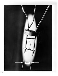
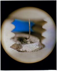
In the autumn of 1962, General Electric’s Schenectady and Syracuse facilities, IBM Thomas J. Watson Research Center, and MIT Lincoln Laboratory each independently reported the first demonstrations of the semiconductor laser. Smaller than a grain of rice, powered using direct current injection, and available at wavelengths spanning the ultraviolet to the infrared, the semiconductor laser became ubiquitous in modern communications, data storage, and precision measurement systems.
200-250 word abstract describing the significance of the technical achievement being proposed, the person(s) involved, historical context, humanitarian and social impact, as well as any possible controversies the advocate might need to review.
IEEE technical societies and technical councils within whose fields of interest the Milestone proposal resides.
In what IEEE section(s) does it reside?
Boston Section, New York Section, and Schenectady Section.
IEEE Organizational Unit(s) which have agreed to sponsor the Milestone:
IEEE Organizational Unit(s) paying for milestone plaque(s):
Unit: IEEE Boston
Senior Officer Name: Denise Griffin, 2022 IEEE Boston Section Chair
Unit: IEEE New York
Senior Officer Name: Robert Pellegrino
Unit: IEEE Schenectady
Senior Officer Name: Krishnat Patil
Unit: IEEE Boston
Senior Officer Name: Gilmore Cooke, Boston Section Milestone Coordinator
Unit: IEEE Boston
Senior Officer Name: Robert J. Alongi, Jr., Business Manager
IEEE Organizational Unit(s) arranging the dedication ceremony:
Unit: IEEE Boston
Senior Officer Name: Denise Griffin, 2022 IEEE Boston Section Chair
Unit: IEEE New York
Senior Officer Name: Robert Pellegrino
Unit: IEEE Schenectady
Senior Officer Name: Krishnat Patil
Unit: IEEE Boston Section
Senior Officer Name: Gilmore Cooke, Boston Section Milestone Coordinator
Unit: IEEE Boston Section
Senior Officer Name: Robert J. Alongi, Jr., Business Manager
IEEE section(s) monitoring the plaque(s):
IEEE Section: IEEE Boston
IEEE Section Chair name: Denise Griffin, 2022 IEEE Boston Section Chair
IEEE Section: IEEE New York
IEEE Section Chair name: Robert Pellegrino
IEEE Section: IEEE Schenectady
IEEE Section Chair name: Krishnat Patil
Milestone proposer(s):
Proposer name: Paul Juodawlkis
Proposer email: Proposer's email masked to public
Please note: your email address and contact information will be masked on the website for privacy reasons. Only IEEE History Center Staff will be able to view the email address.
Street address(es) and GPS coordinates in decimal form of the intended milestone plaque site(s):
• K West B Level, North, GE Research, One Research Circle, Niskayuna, NY 12309 (GPS Coordinates: 42.8312° N, 73.8797° W)
• Main Lobby, IBM Thomas J. Watson Research Center, 1101 Kitchawan Road, Yorktown Heights, NY 10598 (GPS coordinates: 41.2098° N, 73.8026° W)
• Main Lobby, Massachusetts Institute of Technology, Lincoln Laboratory, 244 Wood Street, Lexington, MA 02421 (GPS coordinates: 42.459061° N, 71.266997° W)
Describe briefly the intended site(s) of the milestone plaque(s). The intended site(s) must have a direct connection with the achievement (e.g. where developed, invented, tested, demonstrated, installed, or operated, etc.). A museum where a device or example of the technology is displayed, or the university where the inventor studied, are not, in themselves, sufficient connection for a milestone plaque.
Please give the details of the mounting, i.e. on the outside of the building, in the ground floor entrance hall, on a plinth on the grounds, etc. If visitors to the plaque site will need to go through security, or make an appointment, please give the contact information visitors will need.
It is proposed that a plaque be installed at each of the institutions that first demonstrated the semiconductor laser in the fall of 1962:
GE Research Niskayuna and Syracuse - Corporate Building
IBM Thomas J. Watson Research Center - Corporate Building
MIT Lincoln Laboratory - Corporate Building
Are the original buildings extant?
In three of four cases, the original buildings where the semiconductor laser was first demonstrated are extant. In the case of the GE Syracuse site, the building is no longer extant and thus a single plaque at GE Niskayuna will represent both.
Details of the plaque mounting:
• GE Research Niskayuna: The plaque will be mounted on the wall near the semiconductor research laboratories at GE Research. The GE Research site in Niskayuna is where semiconductor lasers where tested, both the GaAs laser Robert Hall’s team developed and the GaAsP visible laser developed in GE Syracuse by Nick Holonyak’s team
• IBM: Structural column in the main lobby of the building
• MIT Lincoln Laboratory: Main Lobby milestone display case, alongside other IEEE Milestone plaques
How is the site protected/secured, and in what ways is it accessible to the public?
• GE Research Niskayuna: The site is gated with security personnel and not open to the general public. Visitors would need to be registered and approved before being allowed on site and must have a GE employee chaperone at all times. Contact to gain access on site: Todd Alhart (518-338-5880)
• IBM: The main lobby is open to the public. To be admitted to the rest of the building, receptionists at the front desk will contact hosts to come to the lobby to escort visitors into the building
• MIT Lincoln Laboratory: The site (MIT Lincoln Laboratory) has gated access that requires presentation of identification to enter. MIT Lincoln Laboratory is a secure facility. The main entrance and lobby area is open to the public, and the Laboratory often opens its auditorium to outside events, including IEEE Boston Section, IEEE Photonics Society Boston Chapter, and IEEE Life Fellow meetings; and Science on Saturday demonstrations for K−12 students.
Who is the present owner of the site(s)?
• GE Research Niskayuna: The General Electric Corporation
• IBM: IBM Corporation
• MIT Lincoln Laboratory: Massachusetts Institute of Technology
What is the historical significance of the work (its technological, scientific, or social importance)? If personal names are included in citation, include detailed support at the end of this section preceded by "Justification for Inclusion of Name(s)". (see section 6 of Milestone Guidelines)
Sixty years after its invention, the semiconductor laser has become a foundational element in a vast range of human endeavors, including optical communications (e.g., transcontinental undersea fiber-optic cables, data-center interconnects, free-space links connecting ground, air, and space), data storage and retrieval (e.g., compact disks [CDs] and digital video disks [DVDs]), human-machine interactions (e.g., computer-mouse pointing devices, laser pointers, printers, and light displays), manufacturing (e.g., industrial cutting and welding), medicine (e.g., optical coherence tomography [OCT]), and even in our leisure activities in the form of children’s toys and displays. Perhaps nowhere else has the semiconductor laser had greater impact than in communications, where every second, a semiconductor laser quietly encodes the sum of human knowledge into light, enabling it to be shared almost instantaneously across oceans and space. This capability is possible at tremendous scale and economy because the semiconductor laser realizes all the elements of a laser – light generation and amplification, lenses, and mirrors – within a solid microminiature block of material.
The enabling characteristics of the semiconductor laser include its small size (i.e., typically less than a cubic millimeter), its efficiency at converting electrical energy into coherent laser light, and its availability in a wide range of colors (or wavelengths) across the spectrum from ultraviolet (UV) to long-wave infrared (LWIR) to terahertz (THz). These desirable attributes attracted the imagination of scientists and engineers who, through decades of innovation, transformed the initial comparatively feeble semiconductor laser into the society-underpinning technology it is today. Still, the semiconductor laser’s potential is not fully tapped, as it is continually used to explore and exploit the realm of quantum mechanics in the service of mankind.

What obstacles (technical, political, geographic) needed to be overcome?
The realization of the semiconductor laser required decades of collaboration between theorists, mathematicians, materials scientists, engineers, and technicians. At the time the theoretical quantum mechanics underpinning the semiconductor laser was set down in the early twentieth century, very little of the materials science knowledge required to make the semiconductor laser existed. This situation changed rapidly after the invention of the semiconductor transistor in 1948.
Spurred by the semiconductor transistor’s success, several corporate and government laboratories had at hand the fertile mix of minds and technology necessary to realize the semiconductor laser. When it was reported at professional society meetings in summer 1962 that nearly 100% of the electrical energy injected into a gallium arsenide semiconductor could be converted into light, several research groups were poised to translate this knowledge into a working semiconductor laser. Within the span of roughly one month in fall 1962, the first semiconductor lasers were independently demonstrated at four research institutions. Following these seminal demonstrations, the concept was quickly replicated and expanded upon in research laboratories worldwide.
What features set this work apart from similar achievements?
In the few years between the demonstrations of the first laser (1960) and the semiconductor laser (1962), lasers could only be realized by an assembly of multiple discrete components, including an optical gain medium (e.g., doped glasses and crystals, atomic and molecular gases) that generated and amplified the light, a “pump” mechanism that energized the gain medium (e.g., flash lamp, electric discharge), and optical elements (e.g., mirrors, waveguides) that guided light and created a resonant cavity. In contrast, semiconductor materials could convert electrical energy directly into light, realizing both functionalities of the gain medium and pump in a single component. Moreover, the additional structures required to create a laser – optics for guiding the light and mirrors for the formation of a resonant cavity – could also be realized within the semiconductor material.
Because all this functionality came together in a tiny volume (less than 1 mm3), it could be economically produced in high volume. And in contrast to preceding laser technologies that were limited to fixed discrete colors (or wavelengths), the alloys making up the semiconductor material could be continuously varied in composition to create a wide range of laser colors, allowing the semiconductor laser to address many different applications within the same fundamental structure.

.
Why was the achievement successful and impactful?
Supporting texts and citations to establish the dates, location, and importance of the achievement: Minimum of five (5), but as many as needed to support the milestone, such as patents, contemporary newspaper articles, journal articles, or chapters in scholarly books. 'Scholarly' is defined as peer-reviewed, with references, and published. You must supply the texts or excerpts themselves, not just the references. At least one of the references must be from a scholarly book or journal article. All supporting materials must be in English, or accompanied by an English translation.
[1] R. N. Hall, G. E. Fenner, J. D. Kingsley, T. J. Soltys, and R. O. Carlson, “Coherent light emission from GaAs junctions,” Phys. Rev. Lett., v. 9, p. 366, 1962. Media:Hall_CoherentLightEmissionFromGaAsJunctions_PhysRevLett9p366_1962.pdf
[2] M. I. Nathan, W. P. Dumke, G. Burns, F. H. Dill, Jr., and G. Lasher, “Stimulated emission of radiation from GaAs p-n junctions,” Appl. Phys. Lett., v. 1, p. 62, 1962. Media: Nathan_StimulatedLightEmissionfFromGaAsJunctions_APL1p62_1962.pdf
[3] N. Holonyak, Jr., and S. F. Bevacqua, “Coherent (visible) light emission from Ga(As1-xPx) junctions,” Appl. Phys. Lett., v. 1, p. 82, 1962. Media: Holonyak_CoherentVisibleLightEmissionFromGaAsPJunctions_APL1p82_1962.pdf
[4] T. M. Quist, R. H. Rediker, R. J. Keyes, W. E. Krag, B. Lax, A. L. McWhorter, H. J. Zeigler, “Semiconductor maser of GaAs,“ Appl. Phys. Lett, v. 1, p. 91, 1962. Media: Quist_SemiconductorMASERofGaAs_APL1p91_1962.pdf
[5] “Two Concerns Make Same Discovery,” The New York Times, November 1, 1962. Media:NYT_semiconductor_laser_article_621101.pdf
[6] R.N. Hall, "Injection Lasers," IEEE JOURNAL OF QUANTUM ELECTRONICS, VOL. QE-23. NO. 6, June1987. Media:Hall_InjectionLasers_JQE23p674_1987.pdf
[7] M.I. Nathan, "Invention of the Injection Laser at IBM," IEEE JOURNAL OF QUANTUM ELECTRONICS, VOL. QE-23, NO. 6, JUNE 1987.Media:Nathan_Invention_of_the_injection_laser_at_IBM_JQE23p679_1987.pdf
[8] N. Holonyak, "Semiconductor Alloy Lasers - 1962," IEEE JOURNAL OF QUANTUM ELECTRONICS, VOL. QE-23. NO. 6, JUNE 1987. Media:Holonyak_SemiconductorAlloyLasers_JQE23p684_1987.pdf
[9] R.H. Redicker, "Research at Lincoln Laboratory Leading upto the Development of the Injection Laser in 1962," IEEE JOURNAL OF QUANTUM ELECTRONICS. VOL. QE-21. NO. 6, JUNE 1987. Media:Rediker_Research_at_Lincoln_laboratory_leading_up_to_the_development_of_the_injection_laser_in_1962_JQE23p692_1987.pdf
Supporting materials (supported formats: GIF, JPEG, PNG, PDF, DOC): All supporting materials must be in English, or if not in English, accompanied by an English translation. You must supply the texts or excerpts themselves, not just the references. For documents that are copyright-encumbered, or which you do not have rights to post, email the documents themselves to ieee-history@ieee.org. Please see the Milestone Program Guidelines for more information.
Supporting Material:
Letter of support from IBM:
Media: IBM_Research_Support_Letter_IEEE_Milestone_Joint_Invention_of_the_Semiconductor_Laser.pdf
Letter of support from New York IEEE Section
Media: IBM_NewYorkSectionLetter_Support_IEEE_Milestone_Invention_of_Laser_Aug_25_2022.doc
Letter of support from MIT Lincoln Laboratory
Media: MIT_LL_Support_Letter_IEEE_Milestone_Joint_Invention_of_the_Semiconductor_Laser.pdf
Letter of support from Boston IEEE Section
Media: MIT_LL_BostonSection_Chair_Support_Letter_IEEE_Milestone_Joint_Invention_of_the_Semiconductor_Laser_v01.doc
Letter of support from President of IEEE Photonics Society, Rene-Jean Essiambre:
Media: Essiambre_IPS_Letter_Support_Milestone_Semiconductor_Lasers_May03_2022.pdf
Please email a jpeg or PDF a letter in English, or with English translation, from the site owner(s) giving permission to place IEEE milestone plaque on the property, and a letter (or forwarded email) from the appropriate Section Chair supporting the Milestone application to ieee-history@ieee.org with the subject line "Attention: Milestone Administrator." Note that there are multiple texts of the letter depending on whether an IEEE organizational unit other than the section will be paying for the plaque(s).
Please recommend reviewers by emailing their names and email addresses to ieee-history@ieee.org. Please include the docket number and brief title of your proposal in the subject line of all emails.
