Milestone-Proposal:Development of Single Chip A-Series Mainframe Processor (SCAMP)
To see comments, or add a comment to this discussion, click here.
Docket #:2025-25
This is a draft proposal, that has not yet been submitted. To submit this proposal, click on the edit button in toolbar above, indicated by an icon displaying a pencil on paper. At the bottom of the form, check the box that says "Submit this proposal to the IEEE History Committee for review. Only check this when the proposal is finished" and save the page.
To the proposer’s knowledge, is this achievement subject to litigation? No
Is the achievement you are proposing more than 25 years old? Yes
Is the achievement you are proposing within IEEE’s designated fields as defined by IEEE Bylaw I-104.11, namely: Engineering, Computer Sciences and Information Technology, Physical Sciences, Biological and Medical Sciences, Mathematics, Technical Communications, Education, Management, and Law and Policy. Yes
Did the achievement provide a meaningful benefit for humanity? Yes
Was it of at least regional importance? Yes
Has an IEEE Organizational Unit agreed to pay for the milestone plaque(s)? Yes
Has the IEEE Section(s) in which the plaque(s) will be located agreed to arrange the dedication ceremony? Yes
Has the IEEE Section in which the milestone is located agreed to take responsibility for the plaque after it is dedicated? Yes
Has the owner of the site agreed to have it designated as an IEEE Milestone? No
Year or range of years in which the achievement occurred:
1985-1989
Title of the proposed milestone:
Development of Single Chip A-Series Mainframe Processor (SCAMP), 1985-1989
Plaque citation summarizing the achievement and its significance; if personal name(s) are included, such name(s) must follow the achievement itself in the citation wording: Text absolutely limited by plaque dimensions to 70 words; 60 is preferable for aesthetic reasons.
In July 1987, Unisys fabricated the first single chip version of the A-series CPU, referred to as SCAMP (Single Chip A-series Mainframe Processor). Utilizing advanced system design, physical design, silicon test and memory packaging technologies, this groundbreaking architecture packaged the entire A-series architecture in a single module. SCAMP enabled the creation of a mainframe computer, delivering power/performance, resilience, scalability and maintainability in a PC desktop form factor.
200-250 word abstract describing the significance of the technical achievement being proposed, the person(s) involved, historical context, humanitarian and social impact, as well as any possible controversies the advocate might need to review.
IEEE technical societies and technical councils within whose fields of interest the Milestone proposal resides.
IEEE FD GLobal Semiconductors, TA Societies (those related to semiconductors, including Computer, EPS, CEDA, EPS, SSCS)
In what IEEE section(s) does it reside?
San Diego
IEEE Organizational Unit(s) which have agreed to sponsor the Milestone:
IEEE Organizational Unit(s) paying for milestone plaque(s):
Unit: San Diego Section
Senior Officer Name: Upal Mahbub
IEEE Organizational Unit(s) arranging the dedication ceremony:
Unit: San Diego Section
Senior Officer Name: Kathy Hayashi
IEEE section(s) monitoring the plaque(s):
IEEE Section: San Diego Section
IEEE Section Chair name: Upal Mahbub
Milestone proposer(s):
Proposer name: Kathy Herring Hayashi
Proposer email: Proposer's email masked to public
Please note: your email address and contact information will be masked on the website for privacy reasons. Only IEEE History Center Staff will be able to view the email address.
Street address(es) and GPS coordinates in decimal form of the intended milestone plaque site(s):
In the vicinity of the main entrance parking lot of the headquarters of former Unisys offices (currently Petco) at 10850 Via Frontera, San Diego, CA 92128 (33.014539 °N -117.097277°W)
Describe briefly the intended site(s) of the milestone plaque(s). The intended site(s) must have a direct connection with the achievement (e.g. where developed, invented, tested, demonstrated, installed, or operated, etc.). A museum where a device or example of the technology is displayed, or the university where the inventor studied, are not, in themselves, sufficient connection for a milestone plaque.
Please give the details of the mounting, i.e. on the outside of the building, in the ground floor entrance hall, on a plinth on the grounds, etc. If visitors to the plaque site will need to go through security, or make an appointment, please give the contact information visitors will need. The facility was the previous headquarters of the Unisys Rancho Bernardo site which housed over 300 employees that worked in engineering design, including CAD, Memory, Test and a prototype fab facility. The actual SCAMP chip was architected, designed, tested and made at the prototype fab at this facility. It is located in a high tech area of Rancho Bernardo that is well populated and has a direct lineage to the work done by the inventors. There are not any other historical markers already on the site.
Are the original buildings extant?
Yes, the building still exists at 10850 Via Frontera, San Diego CA 92128 that was populated by Unisys in 1982 until 2017. The location is currently occupied by a new tenant, Petco.
Details of the plaque mounting:
TBD
How is the site protected/secured, and in what ways is it accessible to the public?
TBD
Who is the present owner of the site(s)?
Petco, Inc., owns all of the buildings at its headquarters.
What is the historical significance of the work (its technological, scientific, or social importance)? If personal names are included in citation, include detailed support at the end of this section preceded by "Justification for Inclusion of Name(s)". (see section 6 of Milestone Guidelines)
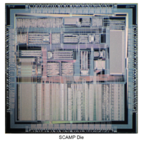
The SCAMP (Single Chip A-series Mainframe Processor) project was the first implementation of Unisys A-series mainframe processor on a single chip This development was innovative in both the architecture itself and the design process used to develop the design. SCAMP was initiated by Burroughs Corporation in November, 1985. A team of systems design engineers from Scotland were sent to collaborate with CAD and physical design teams in the company’s Rancho Bernardo site. The project had dual goals of:
1. Design and fabricate an implementation of the A-Series architecture that was contained on a single C-MOS chip.
2. Use this implementation to create a silicon design system that could be reused on future projects achieving significantly increased capacity over current state-of -the-art capabilities.
What obstacles (technical, political, geographic) needed to be overcome?
In addition to the overall challenge of creating an entire A-Series mainframe on a chip, with Moore's Law driving the industry, many new tools and design challenges would need to be overcome to achieve the design. Industry CAD tools were just being developed, HDL standards and tools were emerging and collaboration between global teams would need to be enabled. SCAMP was a major project, a golden chip that was going to drive state of the art architecture designs and processes which would be needed in order to accomplish this herculean project, and would later help to set the standards for the overall semiconductor industry.
International Assignment The SCAMP team was formed by combining a team on international assignment from Scotland with local teams in the US. This required the Scottish engineers to adapt to new working and home environments. Early in the project two of these engineers decided to return to Scotland and were replaced by other engineers from Scotland. The team had a dual reporting structure, reporting to the local Director in addition to the management in Scotland. This added a burden of travel and reporting that distracted from the program execution. With the closure of the Cumbernauld site the Scottish team had to decide whether to return home or stay to complete the program. Two engineers chose to return home and were replaced with local engineers. The remaining Scottish team members also had to return to Scotland for a period to settle their affairs and clear out their workspace in Cumbernauld. Again these activities distracted from the project work.(2)
Technical Challenges The SCAMP project had to overcome significant technical challenges in order to achieve the program objectives.
1. Getting a full A-Series design that fit in a single, manufacturable semiconductor chip was a major challenge. This was attacked on two fronts. Firstly, the original design was simplified, where possible, to minimize the gate count. The prior implementation occupied 16 bipolar gate arrays (maximum capacity of 2800 gates each) and the final SCAMP module contained 10.3 Million transistors. The SCAMP die contained 100k+ transistors. Secondly, the design system that was developed to implement the SCAMP was able to successfully manage the large design complexity. The previous Lattice based design system could manage a maximum design of ~12 thousand transistors.
2. The SCAMP design system was created by integrating tools that were being developed internally, early adoption of externally developed tools and existing tools. Internally developed tools including the MDS system, Primetime, SWIM, and TDS. Note that the Unisys Primetime tool was an internally developed static timing analysis tool that was developed independent of the Synopsys Inc. PrimeTime tool. Externally developed tools included the Seattle Silicon design tool suite. The early adoption of these tools meant that many issues were uncovered by the SCAMP design that required bug fixes and rerunning the tool once a fix was released. In some instances the SCAMP design itself had to be altered to work around tool issues. There were also delays in the design flow as the team waited for these tool fixes to be released.
3. The adoption of Built-In Self Test as a test methodology was another risk to the SCAMP project. Built-In Self Test was a research subject at the University of Manchester (7) in England and this research provided a starting point for the SCAMP test engineers. There were no test tools that directly supported Self Test so these had to be created concurrent with the design.Defining the appropriate test pattern characteristics for each functional block were not always intuitive and often required a time consuming, trial and error approach.
4. The adoption of a Multi Chip Package for the SCAMP was another area of risk to the SCAMP project. The eleven chip module was larger than previous module designs and the packaging of a logic die and RAM die was also novel. Prior designs contained either logic or RAM die not both. The incorporation of Logic and RAM die in a single module created more complex interconnects. Also, in SCAMP, the SCAMP to RAM connections are in the critical timing path and so these interconnects are highly sensitive. (13)
What features set this work apart from similar achievements?
The SCAMP chip represented many firsts:
The first implementation of a mainframe computer architecture on a single silicon die. This significantly reduced the physical size, power and cooling requirements of an A-Series processor making a PC form factor mainframe feasible.
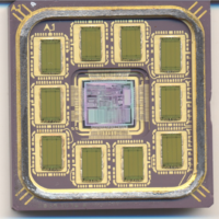
The first implementation of a mainframe computer and associated microcode RAM in a multi chip module. The Multi Chip Module packaging approach ensured that the SCAMP module would achieve competitive performance by reducing the timing path to the microcode RAMs. The MCM package also minimized the PCB area, making a PC AT bus implementation possible. (A requirement for the Micro-A System.
The first mainframe computer that ran processor self test in a system environment. The self test suite developed for the SCAMP enabled the same high functional test suite to be executed at the chip, module, board and system levels for the first time. This provided a significantly higher level of test coverage at the board and system levels than directed tests that would have been used previously.
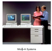
Enabled the first system that supports full mainframe computer functionality in a desktop PC form factor. This lowered the price point for an entry level A-Series system from ~$100,000 to ~$25,000. This enables cost effective configurations of department level systems of up to 16 users . It also supports application development to be performed on the Micro-A, independant of a production A-Series systems. (8), (9), (10).
Design system capacity. When the SCAMP project was initiated the team had been defining the A-5 processor follow-on as a four die CMOS implementation with supporting microcode RAM. This was thought to be achievable if a competitive silicon layout system was adopted. The single die proposal for SCAMP represented a significant stretch goal for the team. The SCAMP design process and tool flow not only achieved the goal for the SCAMP project but was used to produce several generations of SCAMP derivative designs.
Why was the achievement successful and impactful?
Mainframe Computing In the 1980’s Mainframe computers were typically large systems housed in one or more large, refrigerator sized cabinets. These systems often required special power and cooling environments (air conditioned data centers). The Unisys (Burroughs Machines) A -Series mainframe computers were 48 bit, stack based, processors. They ran the proprietary MCP (Master Control Program) operating system that executed the E-Mode instruction set and supported high level languages (e.g. ALGOL, COBOL, Pascal, DMS II, FORTRAN). In the early 1980’s the A5 was the entry level computer in the A-Series range. The processor for this system was implemented using 16 Motorola MCAII ECL gate arrays, each with a maximum capacity of 2800 gates. The gate arrays are mounted on two 23cm x 32 cm printed circuit boards, memory devices and support logic to form the A-Series processor.
Silicon Design Systems Prior to the SCAMP project, reusable silicon layout systems were either gate array based or standard cell based. With a gate array based design a predefined, fixed matrix of identical cells are personalized and interconnected in the metal layers of fabrication. In a standard cell system the design selects functions from a library of standard (fixed height) cells. These are then configured in rows separated by routing channels. The design is then completed by interconnecting the cells using the routing channels. At the start of the SCAMP project Unisys used standard gate arrays for its bi-polar chip developments and a proprietary Lattice layout approach for CMOS designs. The Lattice system consisted of an array of identical sized blocks separated by routing channels. The design was implemented by first partitioning the design into a number of similar sized functions. Each of these functions were then mapped to a physical block and realized using standard cell place and route tools. The design was then completed by globally routing the interconnect between the blocks. While the Lattice layout approach performed well by limiting the number of place-able elements being handled at any one time, it was inefficient in its use of silicon area due to wasted space within the blocks.
SCAMP Design The SCAMP project adopted a block based, hierarchical design approach that partitioned the design into varying sized functional elements that were interconnected to realize the full processor functionality. The design was captured in a custom Hardware Description Language and associated parser called MOD (1]). MOD featured a "module" construct containing three distinct specifications for behavior, structure, and constraints. Using Lisp/AI based frame and template based methodologies, behavior to structure synthesis could be performed by using rules and constraints recursively through the data. Using the Modular Design System (MDS) functionality, the modules were recursively synthesised to create netlists for each of the functional blocks as well as an interconnected netlist for the top level of the design. These designs were then verified for functional and timing correctness at both the block and full chip levels. This provided the needed structural synthesis at a time when existing or commercial tools were not available.
Self Test Design Methodology The SCAMP team executed a comprehensive test strategy to ensure high functional integrity. This strategy began with a detailed functional testability analysis of each architectural block, resulting in the development of targeted test strategies designed to achieve maximum functional coverage. To facilitate efficient test execution and result capture, dedicated test structures were integrated directly into the chip's design. The team further developed the Test Development System (TDS), a specialized tool that streamlined the process of loading test seeds, executing test sequences, and collecting result signatures. Code coverage analysis was then rigorously applied to validate the effectiveness of the developed test vectors, confirming the attainment of target functional coverage. A hybrid approach to test vector generation was implemented, leveraging pseudo-random pattern generators (PRPGs) for broad coverage and directed test vectors (e.g., step patterns, alternating patterns) for targeted fault detection in areas where PRPGs proved insufficient.
This strategy enabled the implementation of cost-effective self-test suites, capable of being executed on low-cost functional test boards, significantly reducing reliance on expensive, multi-million dollar, silicon test systems. Furthermore, these self-test suites were designed for seamless integration into A-Series systems, providing rapid functional verification during system initialization and diagnostic routines.
Drawing on their experience implementing Boundary Scan and Built-In Test methodologies within SCAMP, the test engineers contributed early insights and practical knowledge to the IEEE JTAG Working Group. This group subsequently developed the industry-standard IEEE 1149.1 specification, published in 1990.
SCAMP Physical Design The SCAMP was designed in a 2.5 micron CMOS technology that Unisys licensed from Intel Corporation. It was fabricated in the Unisys captive foundry at the Rancho Bernardo facility. The Scamp physical design was achieved by first creating a target floor plan of the blocks based on each block’s size (gate count), structural complexity and target layout tool. Specific area, aspect ratio and timing budgets were set for each of the blocks based on the top level floor plan. The team were early adopters of Seattle Silicon’s design compiler tools. The standard cell place and route tool (GLUE5) was used for random logic blocks and top level interconnect and a datapath compiler tool (DPATH5) was used for regular datapath functions. A new cell library of datapath cells was created to support the datapath compiler. These cells were fixed height and designed to connect by abutment thus minimizing interconnect between the cells, resulting in a very efficient layout. The datapath compiler works well for regular structures that perform the same functions to each bit of a data bus. The standard cell tool works well for random logic functions. A new design extraction tool was developed at Unisys called SWIM which extracted a switch level netlist from the physical design (GDSII) database. This enabled functional verification of the physical design to ensure no errors were introduced during the layout phase. (3)
SCAMP Multi Chip Module. Traditional A-Series processors were designed with the processor microchips and associated microcode memory RAMs assembled and interconnected on a printed circuit board. The SCAMP project adopted a Multi Chip Module approach where the SCAMP die and associated ten RAM die used to store microcode were mounted on a 2” x 2” multi chip module. This has the dual benefit of significantly reducing the PCB area required to contain the processor while also reducing the length of interconnect between the SCAMP die and microcode RAM. Thus significantly reducing the length of these timing critical paths.
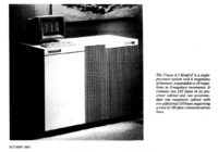
SCAMP based A Series Systems The SCAMP MCM was initially integrated into traditional mainframe cabinets and released as the A1, A4 and A6 systems. These systems supported the full range of A-Series capabilities such as System Expansion, Multi Processing and System Failover. These systems include the A1, A4 and A6. (4), (5), (11), (12).
The SCAMP MCM was one of the enabling technologies for the Micro-A system. The Micro-A’s goal was to integrate A-Series functionality in a desktop PC form factor. The SCAMP module was integrated, along with 12 M bytes of system RAM, DCP (Distributed Communications Controller and SCSI Controller on a single EISA circuit board. This configuration supports full A-Series functionality while dramatically saving Space, Power, Cooling and Cost. (6), (8), (9), (10).
{{
| Milestone | Date |
|---|---|
| SCAMP Project Kick-Off | Nov 1985 |
| Burroughs/Sperry Merger (UNISYS) | Sept 1986 |
| Micro-A Project Kick-Off | Dec 1986 |
| Cumbernauld Site Closure | April 1987 |
| SCAMP-A Prototype | July 1987 |
| Micro-A System Announcement | Jan 1989 |
}}
Supporting texts and citations to establish the dates, location, and importance of the achievement: Minimum of five (5), but as many as needed to support the milestone, such as patents, contemporary newspaper articles, journal articles, or chapters in scholarly books. 'Scholarly' is defined as peer-reviewed, with references, and published. You must supply the texts or excerpts themselves, not just the references. At least one of the references must be from a scholarly book or journal article. All supporting materials must be in English, or accompanied by an English translation.
[1] Computer Science Archive Matty, David Gus. Constraint driven synthesis of hardware design. The University of Utah, 1983, 108 pp. DAI {Sect B} 1984 Jan;44(7):2196. Computer Science.
(2) Daily Times-Advocate (Escondido, California) Team of 8 creates power chip. H1 & H2, Sunday March 19th, 1989.
(3) U.S. Patent 5,315.534 , “Computer process for interconnecting logic circuits utilizing software statements”, Eli S. Schlachet, Issued May 24, 1994.
(4) U.S. Patent 5,574,883i , “Single chip processing unit providing immediate availability of frequently used microcode instruction words” Richard D. Freeman, Issued Nov 12, 1996.
(5) U.S. Patent 5,634,108 , “Single chip processing system utilizing general cace enabling simultaneous multiple functions” Richard D. Freeman, Issued May 27, 1997.
(6) U.S. Patent 5,113,500 , “Multiple cooperating and concurrently operating processors using individually dedicated memories” Jefferson F. Talbott et al, Issued May 12, 1992
(7) Varma, Prabhat. On-Chip Testing of Very Large Scale Integrated Circuits. The University of Manchester, October 1984
(8) The New York Times, Unisys Introduces Micro A Computer, January 19th, 1989
(9) Tech Monitor Unisys Squeezes A-Series CPU Into Desktop Micro, January 18th, 1989
(10) Tech Monitor , Unisys achieves an industry first with it’s Micro 48-Bit mainframe in a desktop enclosure January 24th, 1989
(11) Monitor Unisys SCAMP goes into A4, partitionable A6 mainframes, February 19th, 1990
(12 ) Datapro Research Corporation, Unisys A1, A4 and A6 (New product announcement), December 1987
(13) Multichip Module Technologies and Alternatives, Chapter 14 The Development of Unisys Multichip Modules. 1993.
Supporting materials (supported formats: GIF, JPEG, PNG, PDF, DOC): All supporting materials must be in English, or if not in English, accompanied by an English translation. You must supply the texts or excerpts themselves, not just the references. For documents that are copyright-encumbered, or which you do not have rights to post, email the documents themselves to ieee-history@ieee.org. Please see the Milestone Program Guidelines for more information.
Please email a jpeg or PDF a letter in English, or with English translation, from the site owner(s) giving permission to place IEEE milestone plaque on the property, and a letter (or forwarded email) from the appropriate Section Chair supporting the Milestone application to ieee-history@ieee.org with the subject line "Attention: Milestone Administrator." Note that there are multiple texts of the letter depending on whether an IEEE organizational unit other than the section will be paying for the plaque(s).
Please recommend reviewers by emailing their names and email addresses to ieee-history@ieee.org. Please include the docket number and brief title of your proposal in the subject line of all emails.


