Milestone-Proposal:Bipolar, CMOS and DMOS super integrated technology
To see comments, or add a comment to this discussion, click here.
Docket #:2019-10
This Proposal has been approved, and is now a Milestone
To the proposer’s knowledge, is this achievement subject to litigation? No
Is the achievement you are proposing more than 25 years old? Yes
Is the achievement you are proposing within IEEE’s designated fields as defined by IEEE Bylaw I-104.11, namely: Engineering, Computer Sciences and Information Technology, Physical Sciences, Biological and Medical Sciences, Mathematics, Technical Communications, Education, Management, and Law and Policy. Yes
Did the achievement provide a meaningful benefit for humanity? Yes
Was it of at least regional importance? Yes
Has an IEEE Organizational Unit agreed to pay for the milestone plaque(s)? Yes
Has the IEEE Section(s) in which the plaque(s) will be located agreed to arrange the dedication ceremony? Yes
Has the IEEE Section in which the milestone is located agreed to take responsibility for the plaque after it is dedicated? Yes
Has the owner of the site agreed to have it designated as an IEEE Milestone? Yes
Year or range of years in which the achievement occurred:
1984-1985
Title of the proposed milestone:
Multiple Silicon Technologies on a Chip, 1985
Plaque citation summarizing the achievement and its significance; if personal name(s) are included, such name(s) must follow the achievement itself in the citation wording: Text absolutely limited by plaque dimensions to 70 words; 60 is preferable for aesthetic reasons.
SGS (now STMicroelectronics) pioneered the super-integrated silicon-gate process combining Bipolar, CMOS, and DMOS (BCD) transistors in single chips for complex, power-demanding applications. The first BCD super-integrated circuit, named L6202, was capable of controlling up to 60V-5A at 300 kHz. Subsequent automotive, computer, and industrial applications extensively adopted this process technology, which enabled chip designers flexibly and reliably to combine power, analog, and digital signal processing.
200-250 word abstract describing the significance of the technical achievement being proposed, the person(s) involved, historical context, humanitarian and social impact, as well as any possible controversies the advocate might need to review.
IEEE technical societies and technical councils within whose fields of interest the Milestone proposal resides.
In what IEEE section(s) does it reside?
IEEE Italy Section
IEEE Organizational Unit(s) which have agreed to sponsor the Milestone:
IEEE Organizational Unit(s) paying for milestone plaque(s):
Unit: IEEE Italy Section
Senior Officer Name: Bernardo Tellini
IEEE Organizational Unit(s) arranging the dedication ceremony:
Unit: IEEE Italy Section
Senior Officer Name: Bernardo Tellini
IEEE section(s) monitoring the plaque(s):
IEEE Section: IEEE Italy Section
IEEE Section Chair name: Bernardo Tellini
Milestone proposer(s):
Proposer name: Danilo Pietro Pau
Proposer email: Proposer's email masked to public
Please note: your email address and contact information will be masked on the website for privacy reasons. Only IEEE History Center Staff will be able to view the email address.
Street address(es) and GPS coordinates in decimal form of the intended milestone plaque site(s):
45.571066, 9.363077 and
Describe briefly the intended site(s) of the milestone plaque(s). The intended site(s) must have a direct connection with the achievement (e.g. where developed, invented, tested, demonstrated, installed, or operated, etc.). A museum where a device or example of the technology is displayed, or the university where the inventor studied, are not, in themselves, sufficient connection for a milestone plaque.
Please give the details of the mounting, i.e. on the outside of the building, in the ground floor entrance hall, on a plinth on the grounds, etc. If visitors to the plaque site will need to go through security, or make an appointment, please give the contact information visitors will need. It's the main site for STMicroelectronics Italy where CEO has got the office
Are the original buildings extant?
yes
Details of the plaque mounting:
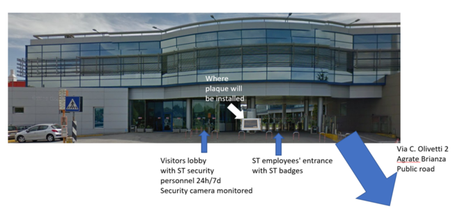
Plaques will be installed in public places at the main entrance as shown below. They will be close to ST security personnel who are is monitoring entrance 24 hours in a day, all days in a year. Very close as indicated there are public roads. Plaque 1: via C. Olivetti 2 Agrate Brianza (Italy) and therefore visitors do not need to be escorted by ST guards to look the plaque or to take a snapshot of it. STMicroelectronics Srl Via C. Olivetti 2, 20864 Agrate Brianza, Italy Google Maps plus code: H9C6+JX. The milestone plaque will be installed right in front of STMicroelectronics Srl Via C. Olivetti 2, 20864 Agrate Brianza, Italy main entrance and lobby. It’s where employees, visitors and customers pass to get in to ST every day. It’s monitored continuously by ST personal 24h/7d by human resources and by security camera. It’s a public place, right outside ST inner perimeter. The site is of premier importance since where ST started with business activities of 55+ years history and culminated in mass-producing BCD devices.
Plaque 2: outside the entrance to the ST building on via Tolomeo 1, Cornaredo, Milan, Italy. 45.470882, 9.034128. The plaque will be mounted on a plinth facing the street. There is a guard post at the entrance who will be able to watch the plaque. This is a public road and therefore visitors do not need to be escorted by ST guards to look the plaque or to take a snapshot of it.
How is the site protected/secured, and in what ways is it accessible to the public?
It’s protected by ST security human resources also with camera, 24h/7d. It’s public and easily accessibile from via C. Olivetti 2 Agrate Brianza, 20864 Italy. It can be easily reached from Linate Airport, close to Milan or from Milan itself.
Who is the present owner of the site(s)?
STMicroelectronics Srl
What is the historical significance of the work (its technological, scientific, or social importance)? If personal names are included in citation, include detailed support at the end of this section preceded by "Justification for Inclusion of Name(s)". (see section 6 of Milestone Guidelines)
Summary of objectives and vision
Key objectives, that motivated STMicroelectronics (short name ST) Silicon Gate Multipower BCD technology development on early 80’s and onward, were:
1) To create a technology integrating heterogeneous transistors and diodes capable to deliver electric power in the range of hundreds Watts
2) To control such a power with logic, which implementation would scale with Moore law
3) To minimize power consumption thus removing heat-sinks
4) To support precise analog functions
5) To address a broad range of applications with reliable implementations
Summary of achievements
To meet such challenging objectives and long-term technology vision, ST since 1985 developed
1) A new integrated Silicon Gate Multipower BCD [1,2,4,9], that allowed the integration on a single chip of diodes, bipolar linear, complex CMOS logic, and multiple DMOS power functions with complex interconnections. The architecture of the process was chosen to optimize the power part, which generally occupied the most chip area. With the DMOS device, many other signal components have been obtained whose electrical and structural characteristics were in relation to manufacturing process.
2) The first proof was the integrated chip, L6202 operated at 60V, delivering 1.5A, switching power at 300KHz with a complex topology connecting power MOS in a package without heatsink [2, 3, 4, 8, 10, 11, 16, 18 pag 571 12/1986].
3) ST has sold more than 30B devices using ST Silicon Gate Multipower BCD [Slide 29 in ref 17 and ref 15]
Besides, the following characteristics have been achieved in the developed technology:
4) To use very efficient silicon gate isolated power DMOS transistors, having all contacts in the top surface and in place of bipolar power transistors. That gave the freedom to integrate higher number of DMOS transistors connected without constraints in a compact chip [4]. Moreover, Power DMOS shown no driving power in dc condition, and no secondary breakdown limitation.
5) Compatibility with CMOS silicon gate devices, enabling very fast switching speed [1, 4]
6) Integration of complex CMOS logic up to complexity of modern micro controllers following Moore Law (figure 6), (figure 11, [4])
7) Use of DMOS component as Power device secure hundreds output power without high dissipation overcoming high current heating that were obstacles to the miniaturization of power switching [4].
8) Reduced electromagnetic interference and better device reliability
9) Technology modularity by allowing to add further Non-Volatile Memory, Insulation, Galvanic isolation, extended power range to KVs
10) Thanks to the integration of power management, data conversion, processing and actuation functionalities many diversified applications were addressed, such as automotive [20] (engine management, ABS, airbag, ESP, car radio, vehicle electrification, charging stations), computer peripherals (printers, hard drives, wireless charges), phones, micro machines MEMs, bio-medical (ultrasound imaging, echography), consumer, industrial (lighting, displays, powerline modems) etc
Existing implementations
Power ICs were realized by using pure bipolar technologies for the audio amplifier market. These devices, mainly operating in switching mode, were severely limited by the poor efficiency and the thermal run-away effect of bipolar power transistors. This poor efficiency meant that a significant amount of power was dissipated inside the device. Since there was a limited dissipation capacity of an IC package, this represented a limitation on the available delivered power.
Another limitation was the poor density of bipolar logic: with the growing request of logic functions, the I2L approach was no more competitive due to its design complexity, high power consumption and limited shrink capability with the lithography.
Other processes used discrete-type DMOS structures where the lower surface of the die was the drain contact, so that two or more DMOS devices could only be placed on the same chip with the limitation constraint to have a common drain contact. Existing configurations were not feasible for complex connections and numerous power device integration, since featured drain on the bottom of the die where a single or common drain power transistors can be integrated [5]. This limited the freedom to design complex integrated BCD circuits. In [6] the core of the fabrication sequence was a metal gate CMOS process. Using that process, figure 3(b) of [6] shows the photomicrograph of a test chip which complexity was very simple. Other firms were focused on metal gate standard CMOS to which added Power MOS and bipolar. This was another key difference vs ST Silicon Gate power DMOS which was integration friendly with standard CMOS, bipolar transistors and diodes. As matter of fact Silicon Gate Multipower BCD introduced by ST become broadly adopted by many applications pushing the former to niche application. If the former would be used broadly then it couldn’t scale, couldn’t be cheap like the ST technology thus preventing it to be adopted into a broad range of applications like ST technology achieved. Those solutions, with Metal gate Power MOS architecture presented in the early phase of BCD technology had short life and disappeared up to the point today they are no more used and not being compatible with CMOS silicon gate evolution.
ST innovations
ST innovated combining on 1984 DMOS/CMOS/Bipolar/Diodes technologies [2]. Silicon Gate Multipower DMOS devices were the best way to manage high power in a monolithic system: in fact, they exhibited technological compatibility with silicon gate CMOS, very fast switching speed, no driving power in dc condition and no secondary breakdown limitation. Since DMOS power stage had intrinsic recirculation diode, no external discrete diodes were needed, saving components [1,2,4,9]. Technology compatibility with Silicon Gate CMOS secured very high-density signal circuits. At the same time high precision analog performance were provided integrating bipolar transistors.
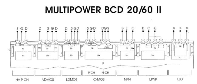
This technology allowed the integration on the same chip of more power DMOS devices isolated from each other, together with Silicon gate CMOS and Bipolar transistors (fig.2), having all the contacts on the top surface. With ST Silicon gate Multipower BCD, hardware designers were free for the first time to integrate any number of DMOS power transistors connected in any way including bridge configurations as said in [4]. Differently to metal gate, ST chose self-aligning silicon gate to achieve logic scaling with Moore law. As result ST first implementation L6202 shown in figure 6 [1], figure 2 in [4], figure 4 in [8] was more complex and sophisticated vs the existing in figure 3(b) in [6].
Figure 2 Notice combined vertical DMOS and junction isolated technologies.
Since DMOS transistors are fully isolated and have all contacts on the top surface any kind of power stage can be integrated
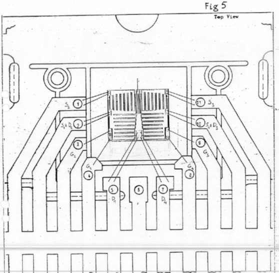
At the same time ST worked on proving the technology with hardware implementations. On 1984 the first power MOS chip has been developed and was reliably working in the range of 60V, with four Power DMOS connected in H bridge configuration (Fig.3 project code name was B4309, see internal report [7] and [2]).
Fig.3 four Isolated 60V H Bridge Power DMOS integrated in a single chip
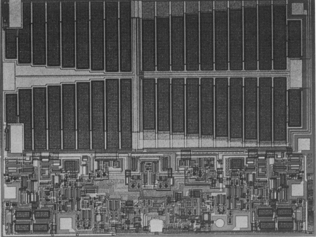
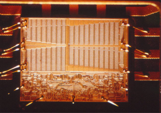
Next on 1985 [1, 3, 8, 9, 10, 11, 16] ST, developed the first integrated circuit: a switching bridge control system for DC and stepping motors (60V, 5A) working at 300KHz with high efficiency. It used Silicon gate Multipower BCD technology just created. The powerful, monolithic integrated circuit was named L6202, internal code name U002 (figure 4). Since the power dissipation was only 1.5W when the output current was 1.5A, the device was working at this level in a standard D.I.P. package with great advantages in terms of cost (no heatsink) and compactness.
Figure 4 L6202, internal code name U002, die photograph
At the same time ST designed for comparison a bipolar bridge with identical power performances [4]. Both chips operated on 48V supplies and delivered 1.5A continuous output current. But while L6202 was assembled in a DIP package and needed no heatsink, its bipolar counterpart needed a power package and a hefty heatsink. Eliminating this heatsink by L6202 was a great demonstration of the importance of reduced dissipation in power ICs. Patent was also granted [ref. Patents 1, US 4,949,142].
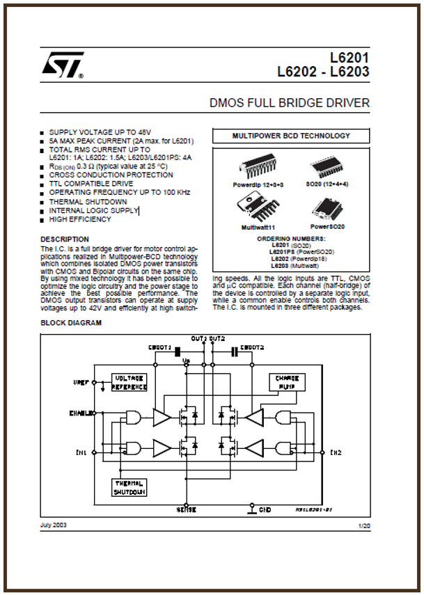
This IC is still in production today, same name, after 35 years as well as many its derivatives [12].
On 1987 ST Silicon gate Multipower BCD technology was chosen by a top Car parts manufacturer [20] to address ICs for Automotive applications in the field of Power Train, Safety and Body. This cooperation is still running after 33+ years [13, 14]
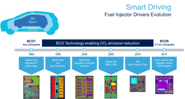
Figure 5 BCD evolution 1993 to 2015 for automotive reduced emissions
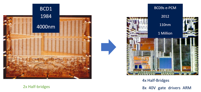
The ST Silicon gate multipower BCD integrated process secured compatibility with CMOS evolution according to Moore law giving, till today, the possibility to realize complex Smart Power systems integrating far more complex microprocessors, Non-Volatile Memories (NVM), and precise analog function (figure 5, 6).
Figure 6 : Motor Control evolution: from the simplest architecture (1 Full bridge in BCD1, left side) to the Full system integration (2 Full bridges, 6 external Power drivers, ARM micro controller CortexM4 with 32 Kbytes NVM based on PCM, phase change memories, right side) in a smaller silicon area
All along the years Silicon gate Multipower BCD technology has confirmed its flexibility to differentiation, voltage capability extended up to 1200V, compatibility with various solutions of NVM, precise passive components (Thin Film Resistor, etc.) and recently even integration of Galvanic isolation (6KV) That has widened the application fields: industrial, cellular, car electrification, many others. with more than 30B units delivered on the market by ST [15]
ST Silicon gate multipower BCD technology guaranteed 30+ manufacturing life of products, and longer life of otherwise obsolete 6” and 8” CMOS fabs. Currently ST is building 12” modern fab to sustain evolution. All those fabs created strong social and labor impact on many employees and relative family’s lives with a sustainable environmental impact.
What obstacles (technical, political, geographic) needed to be overcome?
Ⅰ. Technology wise:
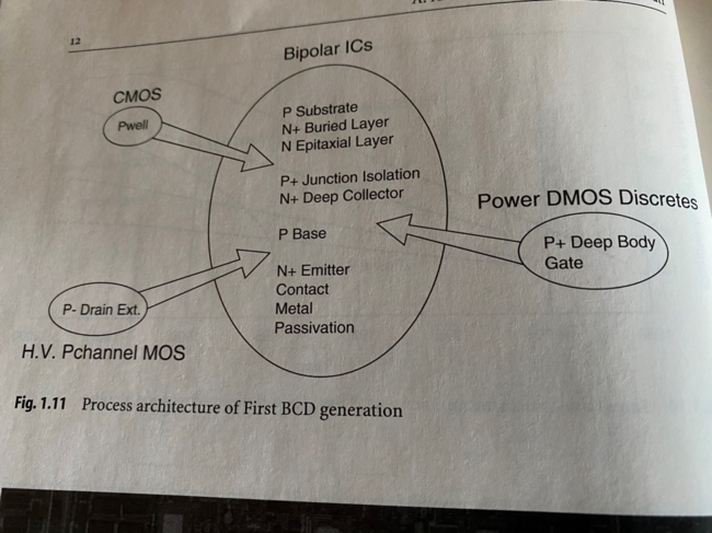
1) ST needed to overcome the integration of different technologies, transistors (fig. 7) and setup manufacturing process and machines each one engineered for a different objective. Originally the architecture of the first ST BCD generation, designed at 4um, had to integrate the Vertical DMOS silicon gate process and the junction isolation technique Vertical DMOS structure with the Power discrete structures with the availability of some key modules (buried layer, epi and sinker) from Bipolar technology. Wafers needed to be processed in 2 manufacturing plants (Cornaredo, for bipolar integrated devices and Agrate Brianza, for CMOS integrated devices, both in Milan area, north Italy) to achieve integration between Bipolar and CMOS processes. Those components were also combined by adopting the same doping profiles present for DMOS device with a limited number of 11 total masks. In this way at the same time and on the same piece of silicon where present CMOS to implement logic control and bipolar more suitable for analog control. The silicon gate technology since the beginning on top of gate electrode function for CMOS and DMOS it worked also as self-aligned gates, DMOS Field plate, channel stopper, electric shield and interconnection. Thanks to the modular approach of Silicon gate multipower BCD process it was possible adding masks, process steps, extra active (HV p-Ch MOS) and passive components. To allow power system integration and to be suitable for a broad wide range of application these technologies had to be flexible and modular.
Figure 7 Process architecture of the first BCD generation
2) Another barrier was the technology race against obsolescence.
Following ST BCD generations where driven by the need to dominate
A. the continuous logic density increase, including the introduction of Non-Volatile Memories in different solutions, thanks to the lithographic shrinkage typical of CMOS roadmap
B. more and more efficient High Voltage and High-Power integration thanks to innovation in power devices architecture.
C. Introduction of new materials and integration solutions such as the usage of thick Copper metallization and new dielectrics to improve current and power capability and robustness to thermomechanical stress.
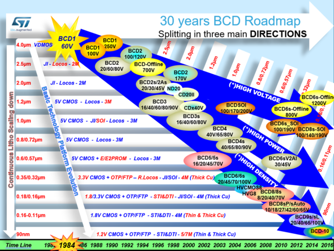
D. differentiation with the introduction of technology options and modules (Junction Isolation, deep trench isolation (DTI), semiconductor on insulator (SOI)) that allowed the improvement of performances or the integration of new functions; like Hall Sensing or Galvanic Isolation or thin film resistors for accuracy. 35 years of ST Silicon gate Multipower BCD technology efforts led to the development of about 10 generations (figure 8), with a lot of differentiation in terms of voltage rating, analog or digital content, Non-Volatile Memory integration, and Power capability.
Figure 8 32+ years of Silicon Gate Multipower BCD evolution since 1984. Note the splitting in the three main directions “High Voltage”, “High Power” and “High Density” because evolving at different speeds respect to lithography scaling down. This has been continuous but at a speed lower than the one of CMOS. Note also the Basic Technology platforms around which the various steps have been designed. The evolution shows the main changes moving from a platform to another one.
As of today, Silicon gate Multipower BCD technologies are available with Voltage Rating spanning from 5V to 1200V, with specific applications like Galvanic Isolation up to 6KV, and lithography features in mass production down to 90nm.
Many applications fields are today covered, and each of them takes benefit from specific technology features that can be added with the best tradeoff between cost and performances.
ST Silicon gate Multipower BCD technologies are characterized by stable and long-term production, given typical application markets like automotive and industrial, exploiting at much manufacturing efficiency and not requiring fast product replacement.
At the same time new emerging applications with specific requirements are fostering the ST technology evolution towards further lithography scaling down to 55nm/40nm, at low voltage (5V to 20V).
Future evolutions are foreseen to exploit heterogeneous integration for improved power devices integration, like Gallium Nitride (GaN) and Silicon on the same chip.
On top of the classical ST Silicon gate Multipower BCD roadmap, following the more than Moore approach, it is important to consider a complementary parallel path alternative to the monolithic integration, that is system in advanced package solutions, like for example embedded die, were different silicon technologies including passive components can provide the best tradeoff between performances and cost in a single package
3) Another barrier was since R&D pre-production products were manufactured with 6-inch wafers while mass production demanded 8-inch ones (and 12” next). Therefore, at the beginning the manufacturing pipelines were quite different, requiring costly re qualification, unification as well as re-training of workforce. Porting and harmonizing from one to another production pipeline were challenging and time consuming. ST researched a technology that had the high-drive advantages of DMOS for power and analog for control by focusing on combining the best of the bipolar circuitry for analog, CMOS for logic, and DMOS power transistors in a harmonized manufacturing pipeline.
4) Existing manufacturing investments. At the beginning Silicon gate Multipower BCD was a niche and power components were considered as discrete components. Moreover, investments were on existing production machines therefore making difficult to replace them with machines suitable for Silicon gate Multipower BCD production. Several product success stories in the automotive and hard disk drive market let barriers to silicon gate multipower BCD adoption to be overcome.
5) departure from the usage of metal gate transistor. The adoption of the technology enabled demonstration of the resulting process on 1984 as a single monolithic device that integrated four 60V power DMOS transistors. That had given birth to the modern Smart Power Integrated Circuit. The first commercial product developed with this technology, the L6202, was a full-bridge motor driver for DC or stepper motors. From this first ST Silicon gate Multipower BCD chip, the technology’s advantages become obvious – and quickly recognized by the experts, while metal gate BCD did not go at the same level of diffusion, adoption and commercial success through the years.
The ST silicon gate power DMOS produced much lower losses and less heat than previous-generation power integrated circuits had been able to achieve. At the same time and on the same piece of silicon, CMOS circuits could implement logic control that had not been practical with bipolar circuitry while continuing to make the bipolar technology and its advantages for analog control available. Integrating the DMOS device onto a Smart Power IC, where engineers could also design the control, was the key to enabling Smart Power actuators for industrial and automotive applications. The lower voltage drops across the DMOS device dramatically reduced power dissipation and produced a higher available output voltage that is critical when operating from 12V batteries, especially in cold cranking applications where the battery voltage can drop to about 6V.
Figure 9 Photomicrograph (colored) of the first integrated L6202 DMOS H-bridge with the control section
Figure 10 L6202 Data Sheet [12], still in production today
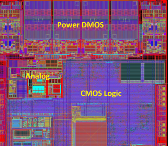
Figure 11 A typical BCD Silicon gate Smart Power device layout, see other examples in [4]
What features set this work apart from similar achievements?
The ST innovation, which has been outlined in this IEEE Milestone proposal and which has significantly advanced the technologies available at that time, can be concisely summarized as follows:
1) The very 1st silicon gate integration of DMOS/CMOS/Bipolar/Diodes on 1984, [2]
2) First proof with L6202 more sophisticated than existing therefore setting the state of art on 1985. [3]
3) Free connectivity of power MOS for the first time [1, 4]
4) High power management with low dissipation and high efficiency [1]
5) Self-aligning silicon gate Power DMOS to secure compatibility with CMOS logic scaling with Moore law, thus allowing micro controllers integration. [1]
6) Modular and scalable technology platform approach open to integrate nonvolatile memories to address diversified applications [1, 4]
7) Very fast switching speed, no driving power in dc condition and no secondary breakdown limitation. [1, 4, 7, 8, 9, 10]
8) No external components needed to achieve low cost and broad adoption [1, 4]
9) High precision analog performance [1]
Why was the achievement successful and impactful?
Supporting texts and citations to establish the dates, location, and importance of the achievement: Minimum of five (5), but as many as needed to support the milestone, such as patents, contemporary newspaper articles, journal articles, or chapters in scholarly books. 'Scholarly' is defined as peer-reviewed, with references, and published. You must supply the texts or excerpts themselves, not just the references. At least one of the references must be from a scholarly book or journal article. All supporting materials must be in English, or accompanied by an English translation.
Publications: Articles, Journals
[1] A New Integrated Silicon Gate Technology Combining Bipolar Linear, CMOS Logic, and DMOS Power Parts A. Andreini, Claudio Contiero and Paola Galbiati, IEEE Transactions on Electron Devices, Vol ED-33, No. 12, December 1986
[2] Single Chip Carries three technologies, Electronics week, ISSN07 48-3252, 1984
[3] Baulemente, Drei Technologien auf einem Chip, Carlo Cini, Claudio Contiero, Petr Hrassky, Elektronik 9/3.5.1985
[4] Mixed Bipolar-Cmos-Dmos Smart Power IC Technology, C. Cini SGS-THOMSON, invited paper 21st International Conference on Microelectronics, MIEL’93; 29th Symposium on Device and Materials, SD’93; Sept 29 – Oct 1, 1993, Bled, Slovenia
[5] Integrated circuits for the control of high power; R.S. Wrathall, D. Tam, L. Terry, S. P. Robb, Motorola
[6] An Analog Technology Integrates BipolarC, MOS, and High-Voltage DMOS Transistors, S. Krishna, J.Kuo, I.S. Gaeta, IEEE TRANSACTIONS ON ELECTKON DEVICES, VOL. ED-31, NO. 1, JANUARY 1984
[7] Technical report No. 01/84, Descrizione Quartina di Power MOS Integrati in configurazione circuitale a Ponte, Agrate March, 21st 1984, C. Contiero, P. Galbiati
[8] A new Bipolar C-MOS, D-MOS, Mixed technology for Intelligent Power Applications, C. Cini, C. Contiero, C. Diazzi, P. Galbiati, D. Rossi, ESSDERC, 1985 Proceedings, Aachen (Germany), September 1985
[9] A New High Frequency, High Efficiency, Mixed Technology Motor Driver I.C., C. Cini ; C. Diazzi ; D. Rossi, ESSCIRC '86: Twelfth European Solid-State Circuits Conference
[10] The Elmer A. Sperry Award to Bruno Murari, 2017
[11] Shortform Semiconductor Products, SGS 1987 with L6202 mention
[12] https://www.st.com/en/motor-drivers/l6202.html ; https://www.st.com/en/motor-drivers/brushed-dc-motor-drivers.html#products
[13] https://investors.st.com/news-releases/news-release-details/stmicroelectronics-licenses-leading-edge-smart-power-process
[14] https://www.eetimes.com/st-bosch-sign-licensing-agreement/#
[15] https://youtu.be/v_z4TO-drag
[16] L6202 SGS Advance Data, 1986
[17] https://investors.st.com/static-files/ba419430-422e-4e99-bb66-38f61ba8e3f3, ref17_Q4 2017 Earnings Release Presentation.pdf
[18] SGS_Motion_Control_Application_Manual, 1987 (L6202 advance data pag 571 12/1986) http://www.bitsavers.org/components/sgs/_dataBooks/1987_SGS_Motion_Control_Application_Manual.pdf
[19] https://investors.st.com/static-files/ba419430-422e-4e99-bb66-38f61ba8e3f3
[20] Bosch Endorsement of STM/BCD technology application for IEEE History Center Milestone Award 2020
Patents:
1. Integrated N-Channel power MOS Bridge Circuit, US4949142A
Supporting materials (supported formats: GIF, JPEG, PNG, PDF, DOC): All supporting materials must be in English, or if not in English, accompanied by an English translation. You must supply the texts or excerpts themselves, not just the references. For documents that are copyright-encumbered, or which you do not have rights to post, email the documents themselves to ieee-history@ieee.org. Please see the Milestone Program Guidelines for more information.
1st patent was INTEGRATED N-CHANNEL POWER MOS BRIDGE CIRCUIT Number 4,949,142 Foreign Application Priority Data Dec. 18, 1984 (IT) Italy. 24.126 A/84
Please email a jpeg or PDF a letter in English, or with English translation, from the site owner(s) giving permission to place IEEE milestone plaque on the property, and a letter (or forwarded email) from the appropriate Section Chair supporting the Milestone application to ieee-history@ieee.org with the subject line "Attention: Milestone Administrator." Note that there are multiple texts of the letter depending on whether an IEEE organizational unit other than the section will be paying for the plaque(s).
Please recommend reviewers by emailing their names and email addresses to ieee-history@ieee.org. Please include the docket number and brief title of your proposal in the subject line of all emails.
