File:Elekiteru-post-museum-schematics.jpg
From IEEE Milestones Wiki
Size of this preview: 737 × 600 pixels. Other resolution: 1,315 × 1,070 pixels.
Original file (1,315 × 1,070 pixels, file size: 157 KB, MIME type: image/jpeg)
Summary
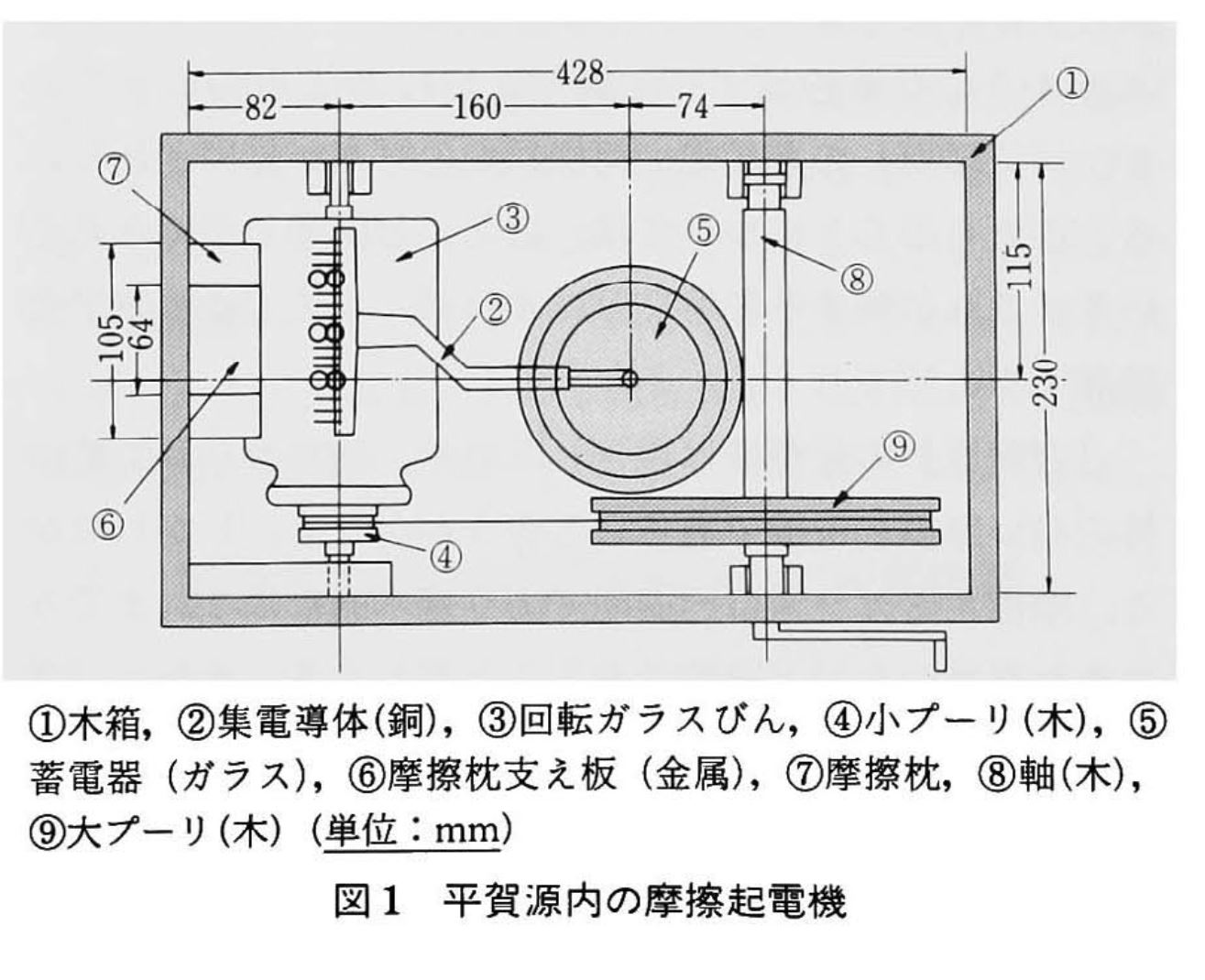
The internal structure of Elekiteru device created by Hiraga Gennai (Hiraga being the family name, and Gennai being given name). This device is displayed at Post Museum in Tokyo, Japan.
Taken from the Figure 1 of 布施光男「江戸時代電気技術はどう培われたか」電学誌115号、1995年
File history
Click on a date/time to view the file as it appeared at that time.
| Date/Time | Thumbnail | Dimensions | User | Comment | |
|---|---|---|---|---|---|
| current | 21:10, 28 April 2024 | | 1,315 × 1,070 (157 KB) | Zephyrus00jp (talk | contribs) | The internal structure of Elekiteru device created by Hiraga Gennai (Hiraga being the family name, and Gennai being given name). This device is displayed at Post Museum in Tokyo, Japan. |
You cannot overwrite this file.
File usage
The following page uses this file: